AUERI NEWS LETTER SPRING 2024
EVOLUTION IN LEAD-FREE SOLDER ALLOYS SUBJECTED TO BOTH MECHANICAL CYCLING AND AGING
Solder joints in electronic packaging frequently encounter failure from cyclic thermo-mechanical loading, especially in demanding environments like automotive engine compartments or industrial power plants. These components undergo both thermal cycling and mechanical cycling due to vibrations, along with thermal stresses from frequent power switching. As a result, the solder materials attaching these electronic components endure cyclic stresses and strains from temperature fluctuations, assembly material mismatches, and dynamic loadings.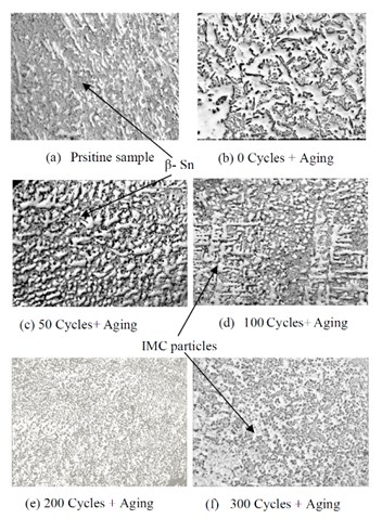
Recent studies by our group have explored the mechanical behavior and property evolution of lead-free solder alloys due to either isothermal aging or isothermal mechanical cycling. Isothermal aging primarily induces microstructure changes, while mechanical cycling involves both microstructural evolution and damage accumulation, such as microcrack growth. However, no prior investigations have explored the combined effects of isothermal aging and mechanical cycling on the mechanical properties and microstructural evolution of lead-free solder alloys.
In this study, uniaxial samples of SAC305 lead-free solder alloy underwent solidification in glass tubes following a controlled reflow profile. The samples experienced mechanical cycling under strain control for various durations, followed by aging for 20 days at 125°C. Nanoindentation testing was then conducted to evaluate mechanical properties, revealing significant deteriorations, especially in samples cycled 300 times followed by aging. Optical microscopy confirmed microstructural coarsening due to the combined effects of mechanical cycling and aging. This research sheds light on the intricate interactions influencing the degradation of elastic modulus, hardness, and creep properties in solder alloys subjected to both aging and mechanical cycling.
PREDICTIVE MODELING OF HIGH-G POTTED ASSEMBLIES WITH FINE PITCH ELECTRONICS AFTER SUSTAINED HIGH-TEMPERATURE EXPOSURE
In the domains of defense and aerospace, electronic components endure intense G shock and thermo-mechanical loads, necessitating paramount reliability in these demanding environments. To enhance the dependability of printed circuit boards (PCBs) in such applications, potting is employed; however, interfacial delamination at the potting/PCB junction remains a predominant failure mode. Over time, the interfacial characteristics of this junction evolve due to prolonged exposure to elevated temperatures, prompting an investigation into the ramifications of such exposure on interface properties.
This study concentrates on scrutinizing the transformation of interfacial properties at the potting/PCB interface in response to high-temperature exposure and the implementation of restraint mechanisms.
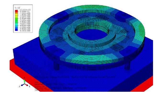
A circular PCB featuring fine-pitch electronic packages and multilayer ceramic chip capacitors is assembled for experimentation. Bimaterial specimens of potting/PCB are fabricated, subjected to four-point bend loading, and examined to determine interfacial fracture toughness properties and cohesive zone parameters. Additionally, potted circular PCBs with various potting materials undergo testing for both pristine conditions and 90-day aging at 150°C. Shock levels of 10,000g and 25,000g are applied to assess the efficacy of potting compounds on the reliability of solder joints in fine-pitch electronics and large discrete components.
This investigation delves into a facet of potting electronics not previously explored, potentially influencing manufacturers. Validated cohesive zone parameters are utilized to devise a predictive finite element high G shock model for circular board assemblies. The experimental conditions are corroborated with the model's output, offering a comprehensive understanding of the potting/PCB interface's interfacial properties. The study also contemplates the prospective application of the predictive model in designing electronic components for harsh environments, providing valuable insights for manufacturers in this specialized field.
EFFECTS OF GRAIN TO SAMPLE VOLUME RATIO ON THE DEFORMATION BEHAVIOR OF POLYCRYSTAL SAC SAMPLES SUBJECTED TO SHEAR LOADS
As electronic components continuously shrink in size, understanding the size effects on the behavior of solder materials in electronic structural components becomes crucial. While extensive studies describe the deformation behavior of bulk SAC (Sn-Ag-Cu) alloys, the impact of size effects on solder deformation in small-scale joints is often overlooked. This study emphasizes the significance of obtaining a constitutive model that accounts for material behavior at smaller scales, particularly considering the increasing miniaturization of solder joints in high-density packaging.
SAC alloys, comprising more than 95% weight percentage of β-Sn, are extensively used for solder interconnects in microelectronic packaging. The anisotropic nature of β-Sn in terms of elastic modulus and coefficient of thermal expansion, along with its crystalline structure, influences plastic deformation through various atomic planes and slip systems. Crystal plasticity theory, implemented through a DAMASK code, is employed to elucidate the mesoscale deformation behavior of polycrystalline beta-tin samples. The study utilizes Voronoi tessellation to generate polycrystalline models with random grain orientations and explores shear simulations for different grain sizes.
The findings reveal that larger grain sizes exhibit isotropic deformation, while smaller grain sizes display anisotropic behavior under shear loads. This investigation sheds light on the critical grain size to sample size ratio where isotropic behavior transitions to anisotropic behavior during shear loading.
COMPARATIVE FINITE ELEMENT ANALYSES OF THE THERMAL CYCLING PERFORMANCES OF BGA PACKAGES WITH SAC, LTS, AND MIXED SAC-LTS SOLDER JOINTS
Understanding the mechanical behavior and reliability of lead-free microelectronic assemblies is crucial, especially for low-melting-point solders like Sn-Bi subjected to thermal cycling. While the industry often relies on the standard SAC (Sn-Ag-Cu) soldering alloy, the increasing use of Sn-Bi solder, with its lower reflow temperature and reduced warpage, emphasizes the need for mechanical characterization.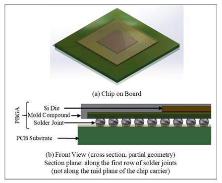
The 42%Sn-58%Bi solder (LTS) is commonly employed in mounting ball grid array (BGA) packages, creating mixed solder joints with SAC solder balls during reflow. Mechanical characterization of these mixed joints under various thermal cycling conditions is vital for predicting electronic package reliability. The study employs quarter-symmetry 3D models representing a plastic BGA package with eutectic Sn-Bi, mixed Sn-Bi/SAC305, and homogeneous SAC305 solder joints. Utilizing Anand parameter coefficients, the models simulate the nonlinear mechanical behaviors of both solders. Thermal cycling between -40 to 125°C is applied to predict thermal fatigue life (TFL) for each solder joint configuration under different PCB surface finishes.
The results indicate that the mixed Sn-Bi/SAC joint exhibits the highest TFL, followed by SAC305, and eutectic Sn-Bi (58Bi-42Sn) joints. Despite failure occurring at the top SMD end, significant plastic work accumulation at the SAC/SnBi interface suggests a nuanced failure mechanism. This study not only estimates TFL but also provides insights into the failure mechanisms of mixed LTS and SAC solder joint configurations under diverse thermal cycling conditions and PCB surface finishes.
SURFACE-MOUNT COMPONENT ATTACHMENT ON AEROSOL JET PRINTED SUSTAINABLE WATER-BASE SILVER NANOPARTICLE INK
Additive methods are preferred over processes that need hard tooling due to ramp-up speed and soft tooling. Increasing demand for the miniaturization of electronics has accelerated the development of flexible electronics technology. Flexible electronic architectures have gained traction in products for various end applications. The prior generation of additive processes used volatile organic solvent-based inks to fabricate printed circuits. Increased emphasis on environmental, social, and governmental factors has called attention to the development of sustainable products. Recent material development has seen the emergence of water-based inks with low-impact environmental waste. Sustainable inks use water as the carrier medium in place of volatile solvents. Owing to the recent introduction of these formulations, less is known about the ability to form functional circuits with sustainable inks or their performance relative to the incumbent non-sustainable volatile organic solvent-based inks.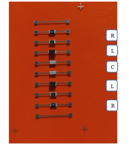
In this paper, components were attached to additively printed water-based ink circuits fabricated using an aerosol jet. Interconnect methods have been studied, including electrically conductive adhesives. The component performance of RLC has been studied as a function of operating frequency and compared with the rated values. Mechanical performance has been studied using the shear load to failure and electron dispersive x-ray spectroscopy. The electrical performance has been correlated with the mechanical performance, and optical methods have also been used to characterize the results of the printed trace.
PROCESS PERFORMANCE INTERACTIONS FOR ADDITIVELY PRINTED WATER-BASED NAOPARTICLE SUSTAINABLE SILVER-INK WITH ULTRASONIC ATOMIZATION ON AEROSOL JET PRINTER
Environmental, social, and governmental factors have received increased attention in the design and manufacture of electronics. Additive printed electronics processes reduce the waste streams from electronics manufacturing by eliminating plate and etch processes, which involve the selective removal of masks and conductive copper to fabricate circuits. In addition, the transition to additive print processes also allows for the elimination of hard tooling, with design changes limited to those that can be implemented quickly, reducing the time involved with design iterations.
The earlier versions of additive inks involved using volatile solvents as carrier mediums for nanoparticle inks. Sustainable inks use water as the carrier medium in place of volatile solvents. Owing to the recent introduction of these formulations, less is known about the ability to form functional circuits with sustainable inks or their performance relative to the incumbent non-sustainable volatile organic solvent-based inks.
In this study, the performance of sustainable water-based solvent inks has been studied and compared with that of volatile solvent inks. The Aerosol Jet printer was used in this work to print and develop process parameters for investigation, including ultrasonic atomizer mass flow rate, sheath flow control, and stage speed, with a water-based sustainable silver nanoparticle ink. Electrical and mechanical properties were tested at various sintering temperatures and times, including resistance and shear load to failure. The results show that the electrical properties are improved by varying these parameters, and optical methods have also been used to characterize the results of the printed trace. Fitted regression models have been developed for process optimization.
INVESTIGATION OF PERFORMANCE AND REPAIRABILITY OF ADDITIVELY PRINTED FUNCTIONAL CIRCUITS WITH WATER-BASED SILVER INK ON AN INKJET PLATFORM
Additive printing techniques, particularly inkjet printing, have gained significant traction in the manufacturing of electronic circuits due to their cost-effective and time-efficient nature. Inkjet printing offers several advantages over traditional methods like screen printing, including the ability to print fine lines and utilize a broader range of conductive inks. Water-based silver ink is an environmentally friendly and highly conductive option. The water-based formulation eliminates the need for toxic solvents, ensuring a safer manufacturing and disposal process.
This research focuses on evaluating the performance of functional circuits additively printed with water-based silver ink using an inkjet platform. The circuits were printed onto a flexible polyimide substrate using an inkjet printer with a piezoelectric printhead. Functional circuits comprising High-Pass and Low-Pass Signal Filters were printed using water-based silver ink, with discrete commercial off-the-shelf (COTS) components attached. The frequency response of these circuits was measured and compared to simulated responses to determine any deviations in electrical performance.
The viability of repairing printed circuits was studied by intentionally detaching and reattaching the components. The repaired circuits were then compared to the pristine circuits in terms of their electrical performance.
DEVELOPMENT AND RELIABILITY EVALUATION OF ADDITIVELY PRINTED BIOSENSING DEVICE FOR WEARABLE APPLICATIONS IN HARSH ENVIRONMENT
Additive technologies have become increasingly favored for producing printed circuit boards (PCBs), eliminating the need for expensive tooling like photomasks or etching containers. The reliance on software-based design and manufacturing not only allows for greater production flexibility but also facilitates quicker tool adjustments and design developments. In contrast to traditional methods that involve subtracting unwanted material from a copper-clad board, additive printing methods can be applied to various fabrics, vehicles, and polymers with different surfaces and forms. This adaptability enables the creation of PCBs designed to fit diverse shapes and surfaces, fostering creativity and versatility in applications.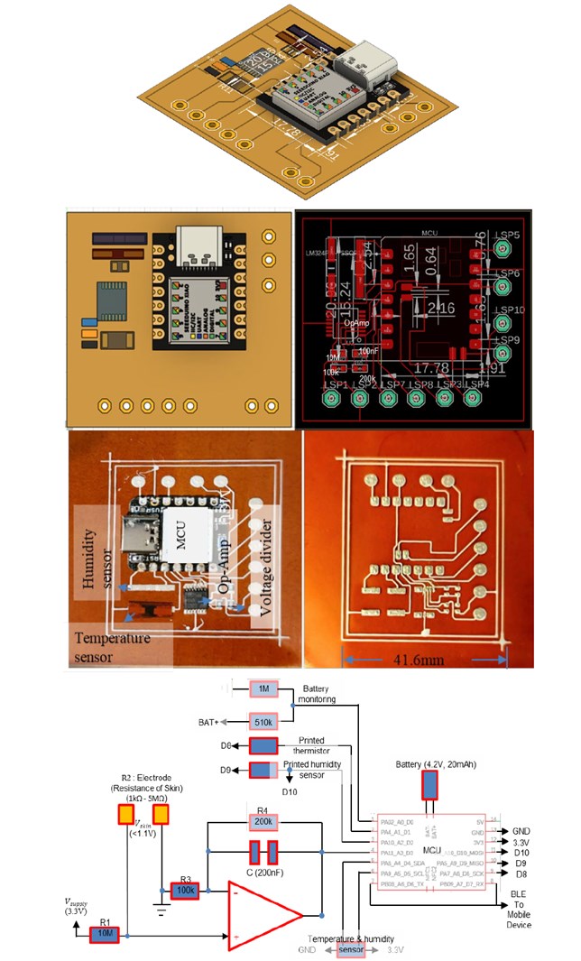
This flexibility extends to applications like wearable biosensors, incorporating an electrocardiography (ECG) sensor, electrodermal activity (EDA) sensor, pulse-oximetric sensor, body temperature sensor, and humidity sensor. These biosensors can monitor various aspects of human health, providing valuable data for medical diagnosis, fitness tracking, and stress management. Despite the potential of additively printed wearable biosensors, challenges related to reliability and durability exist, particularly when subjected to flexing forces and environmental conditions. Addressing stability concerns requires advancements in printing techniques, process recipes, and encapsulation materials.
In this research study, the direct-write (D-write) printing approach was employed to create an integrated wearable biosensor patch. The biosensor features circuits, encapsulations, a body temperature sensor, a humidity sensor, a pulse-oximetric sensor, and an electrodermal activity sensor. Electrically conductive adhesive (ECA) pads were also printed to attach components like a flexible battery, microcontroller, and wireless module. The developed firmware and data acquisition software allow the biosensor to collect and transmit biosignals to mobile devices. The biosensor underwent rigorous testing under varying conditions, demonstrating accuracy, repeatability, stability, sensitivity, linearity, response time, and hysteresis effects for each sensor.
The study contributes to the advancement of sustainable additive manufacturing for healthcare applications, showcasing a reliable and flexible integrated wearable biosensor.
ADDITIVE PRINTING OF WEARABLE EDA SENSORS ON INMOLD ELECTRONICS ON AUTOMOTIVE PLATFORM
Additive manufacturing techniques revolutionize the production of printed circuit boards (PCBs) by eliminating the need for expensive equipment like etching vessels and photomasks. Software-driven design not only ensures production flexibility but also facilitates rapid tool modifications and design enhancements. In contrast to traditional methods requiring complex processes, additive printing methods offer versatility by working on various substrates, vehicles, and polymers with diverse geometries and textures. This newfound flexibility sparks creativity among engineers, enabling the design of innovative applications such as wearable biosensors for monitoring diverse aspects of human health and stress, like the electrodermal activity (EDA) sensor. 
However, concerns arise regarding the stability of current wearable biosensor technology under flexural strain and harsh environmental conditions. To address these challenges, this research study introduces additive fabrication methods for creating PCBs for wearable biosensors without the need for costly equipment or intricate processes. Leveraging the benefits of software-driven design, the focus is on the EDA sensor, designed to measure skin conductance for driver monitoring. Using a direct-write printing technique with an nScrypt printer, the EDA sensor circuits are printed on thermoformable substrates. These substrates, moldable by heat and pressure, enable the PCBs to take various shapes for reliability testing.
The biosensor's performance is rigorously evaluated under different harsh conditions, including thermoformed shapes, temperature, humidity, and human body status, mirroring real-world driving scenarios. The results demonstrate that the additive PCB-based EDA sensor successfully measures skin conductance with acceptable error margins, showcasing mechanical robustness and reliability in diverse conditions. In conclusion, the developed EDA sensor utilizing additive fabrication techniques represents a milestone in monitoring driver stress levels with high reliability and flexibility.
COMPARATIVE STUDY OF SMD COMPONENTS ATTACHED USING ELECTRICALLY CONDUCTIVE ADHESIVE AND MAGNETICALLY ORIENTED ANISOTROPIC CONDUCTIVE ADHESIVE ON INKJET PRINTED STRUCTURES
Due to its high resolution and ability to deposit a variety of functional materials, including conductive inks, insulators, and dielectrics, inkjet printing is a viable method for constructing electronic devices. In this study, the authors sought to examine the electrical and mechanical performance of surface-mounted device (SMD) components mounted on inkjet-printed circuits using two adhesives: Electrically Conductive Adhesive (ECA) and Magnetically Oriented Anisotropic Conductive Adhesive (MOACA). 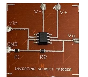
The study is carried out in two phases. In the initial phase, SMD components such as resistors, inductors, and capacitors were mounted using ECA and MOACA on conductive traces with pads, and their electrical performance was compared to their rated values. In the second phase, the behavior of inkjet-printed circuits was studied, including Non-Inverting Amplifier Circuits and Schmitt Trigger Circuits. These functional circuits were constructed on polyimide substrates using silver nanoparticle ink.
Evaluation of the electrical and mechanical performance of the circuits was conducted. Overall, this study provides invaluable insight into the electrical and mechanical behavior of inkjet-printed circuits, particularly in the context of attached components.
LINE WIDTH AND ELECTRICAL PERFORMANCE PREDICTION FOR INKJET PRINTED CONDUCTORS-RESISTORS-INDUCTORS-CAPACITORS
Inkjet printing enables the high-speed production of devices on a variety of substrates while offering an increased level of precision and repeatability. There is a need for closed-loop control over the printing process to achieve geometrical accuracy and consistent electrical performance of printed circuits and components. A sophisticated closed-loop control process can be achieved by establishing a relationship between printer input parameters and the geometrical and electrical outputs of printed objects.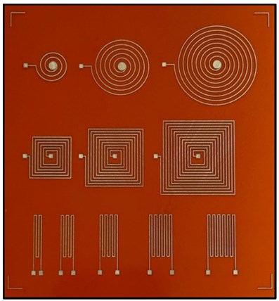
In this study, the impact of various printer settings on the electrical performance and geometrical accuracy of printed circuits and components was examined. Specifically, the effects of print resolution, droplet size, and the number of copies on the electrical performance of printed resistors, planar inductors, and capacitors were investigated. The printing was done using particle-free silver ink on a polyimide substrate.
The statistical model developed from experimental data provides a means of achieving closed-loop control over the printing process, ensuring consistent and accurate production of printed electronic components.
REPARABILITY TEST OF AEROSOL-JET PRINTED SUSTAINABLE SILVER INK CIRCUIT
The earlier generation of additive printable inks was based on volatile organic solvent carrier fluids. Increased awareness of the environmental impact of electronic waste has resulted in the emergence of environmentally friendly water-based inks with low-impact waste. The repairability of additively printed circuits can be used to reduce electronic waste and enable life extensions of deployed electronics through repair and replacement. However, the repairability potential, processes, and impact on reliability are relatively unexplored for new sustainable materials.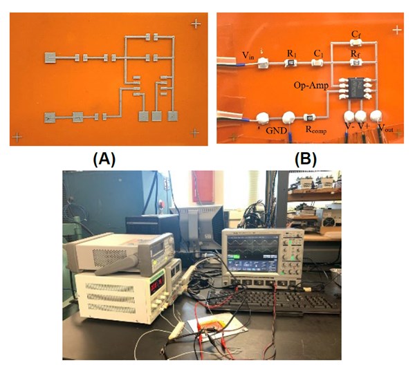
This study consists of a thorough examination of component attachment and the reparability of components on performance and reliability. Repair procedures have been pursued on circuits printed with sustainable conductive ink using an aerosol jet printer (AJP). Adhesives are printed on the pads at the location where the component is to be attached using a direct-write technique capable of printing highly viscous materials such as electrically conductive adhesive (ECA).
The procedure entails attaching a component to a flexible printed circuit, measuring the output response, removing the attached component from the circuit, replacing it with a new component of the same rated value, measuring the output again, and comparing it to the prior output and the simulated output. Furthermore, the mechanical strength of the attached components is characterized in terms of shear load to failure. The force required to remove the attached component using a metal tip before and after the repair is compared for each of the passive components. Finally, a functional differentiator circuit is used to validate the findings.
SUSTAINABLE SILVER INK FLEXIBLE CIRCUITS FABRICATION USING DIRECT WRITE ADDITIVE MANUFACTURING TECHNIQUES
Conventional inorganic inks used to fabricate additive circuits pose a significant environmental challenge due to their toxic nature and non-biodegradable properties. There is a need for a more sustainable alternative for the realization of additively printed electronics. Water-based inks, made from renewable and biodegradable materials, have emerged as a promising solution. 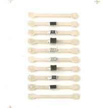
This study focuses on examining process performance interactions for direct-write printed circuits and the attachment of surface-mount components. The authors investigate the ability of direct-write methods to create functional circuits while also exploring the effects of process parameters on the manufactured properties. Process recipes have been developed using a water-based sustainable silver ink applied to two different substrates (PET and Polyimide), and the impact of varying print parameters was compared among the substrates.
The findings reveal the influence of print parameters on the mechanical and electrical properties of the printed traces, as well as demonstrate the additive printing of circuits and the attachment of surface-mount components using the optimal process parameters. Furthermore, the performance of a printed Active Lowpass Filter was evaluated using LTspice software. This research aims to demonstrate the viability of direct-write technology as a sustainable and viable alternative for the manufacture of traditional electronic circuits by successfully attaching surface-mount components to printed pads.
IMPACT OF COMPONENT INTERCONNECTIVITY ON MECHANICAL AND ELECTRICAL PROPERTIES OF FLEXIBLE HYBRID ELECTRONICS WITH PRINTED WATER-BASED SILVER INK CIRCUITS
Flexible Hybrid Electronics (FHE) have the potential to revolutionize the electronics industry by providing sustainable and efficient devices. However, the reliable interconnectivity between printed traces and surface-mount devices (SMD) remains a critical challenge for FHE. There is a need for more research on the use of printed water-based silver ink traces and bonding materials for component attachment in FHE, as the literature on this subject is limited.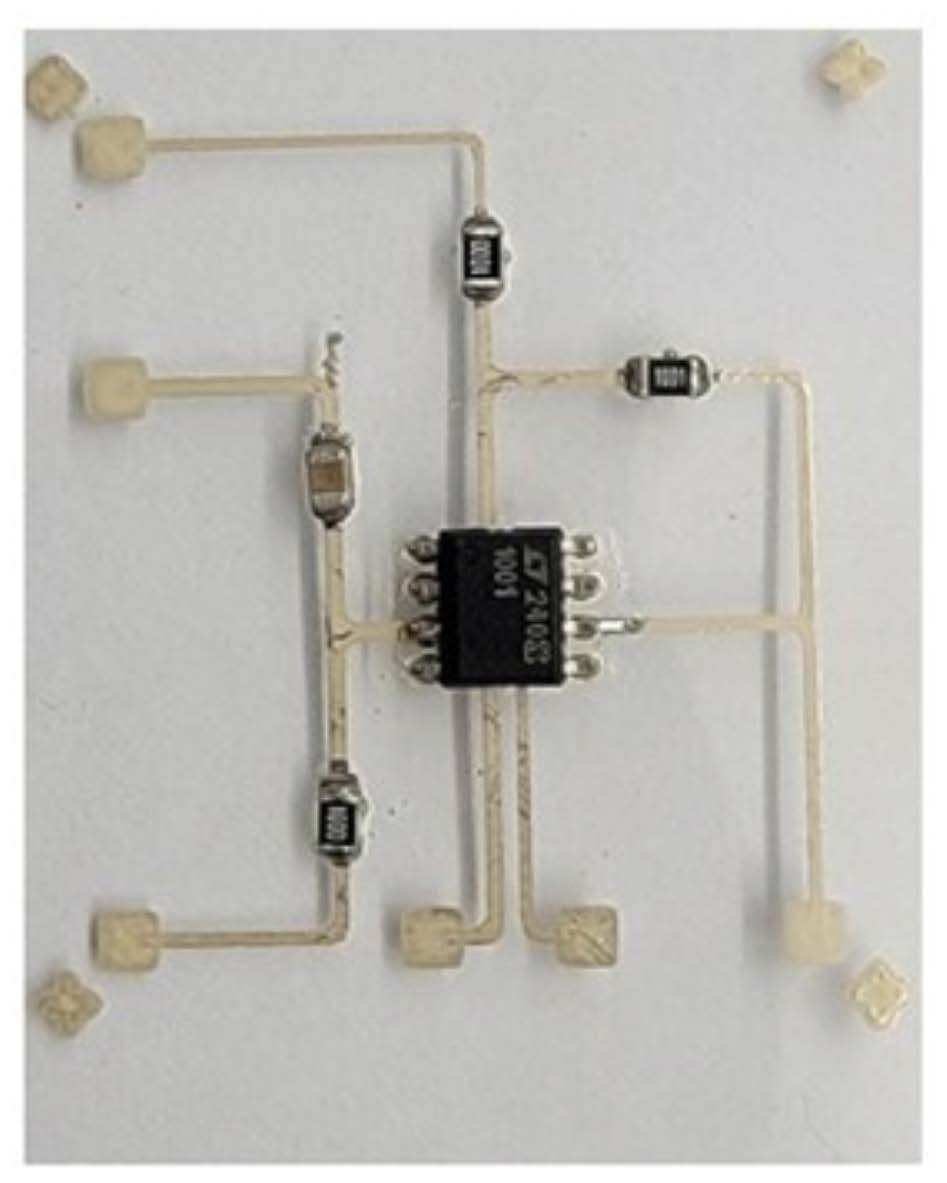
This study was conducted to compare the effects of different bonding materials on component attachment. The bonding materials investigated were electrically conductive adhesive (ECA) and low-temperature solder (LTS). The study used the direct write method to print silver pads, which were then used to attach components such as resistors, inductors, and capacitors using the bonding materials. Electrically conductive adhesive (ECA) results were compared to those of low-temperature solder (LTS).
The interconnectivity of the attached components was evaluated by measuring their rating values before and after attachment. The findings of this study provide insights into the performance of different bonding materials for component attachment in FHE. Such insights can aid in the development of reliable and efficient interconnectivity methods for FHE, which can contribute to the widespread adoption of FHE in various industries.
EFFECT OF SURFACE TREATMENT ON THE FATIGUE CRACK PROPAGATION IN A TIM/COPPER INTERFACE SUBJECTED TO HIGH-TEMPERATURE LONG-TERM EXPOSURE
As electronic devices continue to shrink, effective heat dissipation becomes a critical concern, impacting device reliability. When solid surfaces come into contact, the limited contact area, often only 1% to 2%, results in elevated contact resistance, approximately 100mm²/kW, between bare silicon-to-silicon contacts. To address this issue, thermal interface materials (TIMs) are employed to reduce contact resistance and enhance heat dissipation. Microelectronic packages incorporate multiple bi-material interfaces, influencing device design and reliability.
Dynamic mechanical analysis, such as a 4-point bending test, enables the study of fatigue failure in bi-layer materials. Cyclic loading stress is applied to characterize material fatigue and failure, allowing control over both strain and stress. As semiconductor devices increasingly operate at higher temperatures, reaching 125 – 200°C in high-power density electronics, there is a need for understanding how electronic components endure prolonged exposure to such conditions.
This study assesses the reliability and stability of grounded lid Flip-Chip Ball Grid Array (FCBGA) packages under high-temperature environments. It investigates the low cycle fatigue properties of TIM and copper bi-material interfaces, examining adhesion strength, fracture toughness, and stress intensity factors. The impact of aging time, plasma cleaning power, aging temperatures, and mode-mixity on fatigue crack propagation is explored through the application of Digital Image Correlation (DIC) technology. Paris’ law coefficients and exponents are found to be dependent on mode-mixity, indicating that certain fatigue properties can be derived from monotonic fracture behavior in bi-material interfaces.
COMPARISON OF MACHINE LEARNING APPROACHES FOR CORRELATING PRINT PROCESS PARAMETERS TO REALIZED PHYSICAL AND ELECTRICAL CHARACTERISTICS OF PRINTED ELECTRONICS USING INKJET PLATFORM
In the last decade, printed electronics has gained significant research attention, making inroads into consumer electronics. The key advantage of additive printed electronics lies in its ability to produce lightweight and flexible components at a lower cost than traditional methods. Various printing techniques, conductive inks, dielectrics, solder pastes, and electrically conductive adhesives have been explored to find optimal solutions. However, a common challenge is the disparity between designed and actualized geometrical and electrical characteristics of printed traces, affecting overall circuit performance.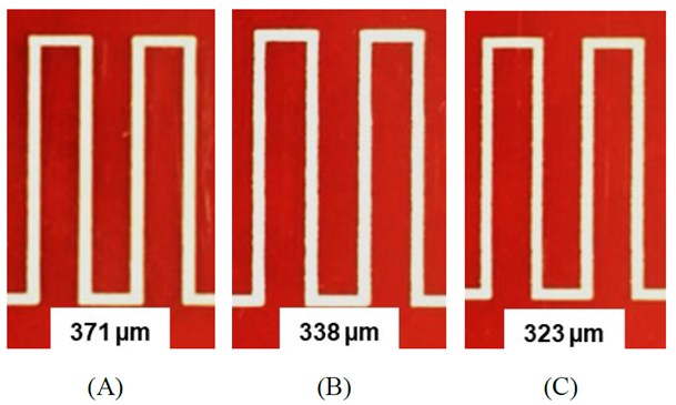
This study focuses on developing a closed-loop control process for adjusting process parameters to achieve desired electrical and physical trace characteristics. Using an inkjet printer and particle-free silver ink, the study establishes a relationship between process parameters and line geometry. Different machine learning methods, including nonlinear regression and Gaussian process regression, are employed and optimized to create a graphical user interface (GUI) for a closed-loop control algorithm. This algorithm provides corrective print parameters based on desired, realized, and current parameters.
EVALUATION OF ADDITIVE CIRCUITS PRINTED WITH SUSTAINABLE AQUEOUS SILVER INKS USING AEROSOL JET PRINTING AND GRAVURE OFFSET PRINTING AND INVESTIGATION OF CIRCUIT REPAIRABILITY
Additive printed electronics, in particular, has been a rapidly advancing field, with applications that span from smart packaging to energy harvesting systems to healthcare devices to intelligent textiles. The basic building block of any flexible circuit created by these technologies is conductive ink. This ink typically comprises metal nanoparticles and several solvents. However, many of the solvents used in these inks are toxic substances or include volatile organic compounds (VOCs) that have a variety of negative effects on the environment and human health, including air pollution, smog, respiratory problems, health risks, and reduced air quality. Consequently, there is a strong push toward developing sustainable materials for use in products, including ink formulations with fewer toxic solvents.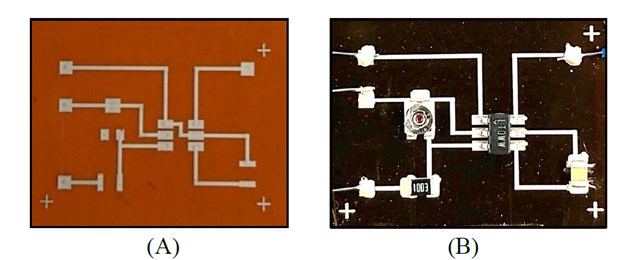
In this study, researchers investigate the use of two printing techniques, aerosol jet printing and gravure offset printing, to print full-wave rectifiers (AC to DC conversion) and voltage bridge oscillators (DC to AC conversion) using commercially available aqueous silver ink. The performance of the additively printed circuits is compared to both theoretical values and to the same circuits printed using non-aqueous inks. Additionally, a switch-mode battery charging circuit has also been printed with a sustainable ink, and its performance has been investigated.
POLARIZATION CURVES, PACKAGE-LEVEL MULTIPHYSICS SIMULATION OF CU85AL15 AND CU94AL6 WB CORROSION FOR AUTOMOTIVE AND RUGGED ENVIRONMENT APPLICATIONS
EVALUATION OF THERMOFORMABILITY OF ADDITIVELY PRINTED CIRCUITS PRINTED USING GRAVURE OFFSET PRINTING TECHNIQUE AND INVESTIGATION OF IN-MOLD ELECTRONIC CIRCUITS
Throughout the past decade, the field of printed electronics has gained increased research impetus and has started to make entryways into the consumer electronics product market. The applications of additive printed electronics are numerous and range from healthcare devices and smart packaging to energy harvesting systems and intelligent textiles. Another novel application area for printed electronics is in-mold electronics (IME), which involves integrating printed electronic circuits into injection-molded parts.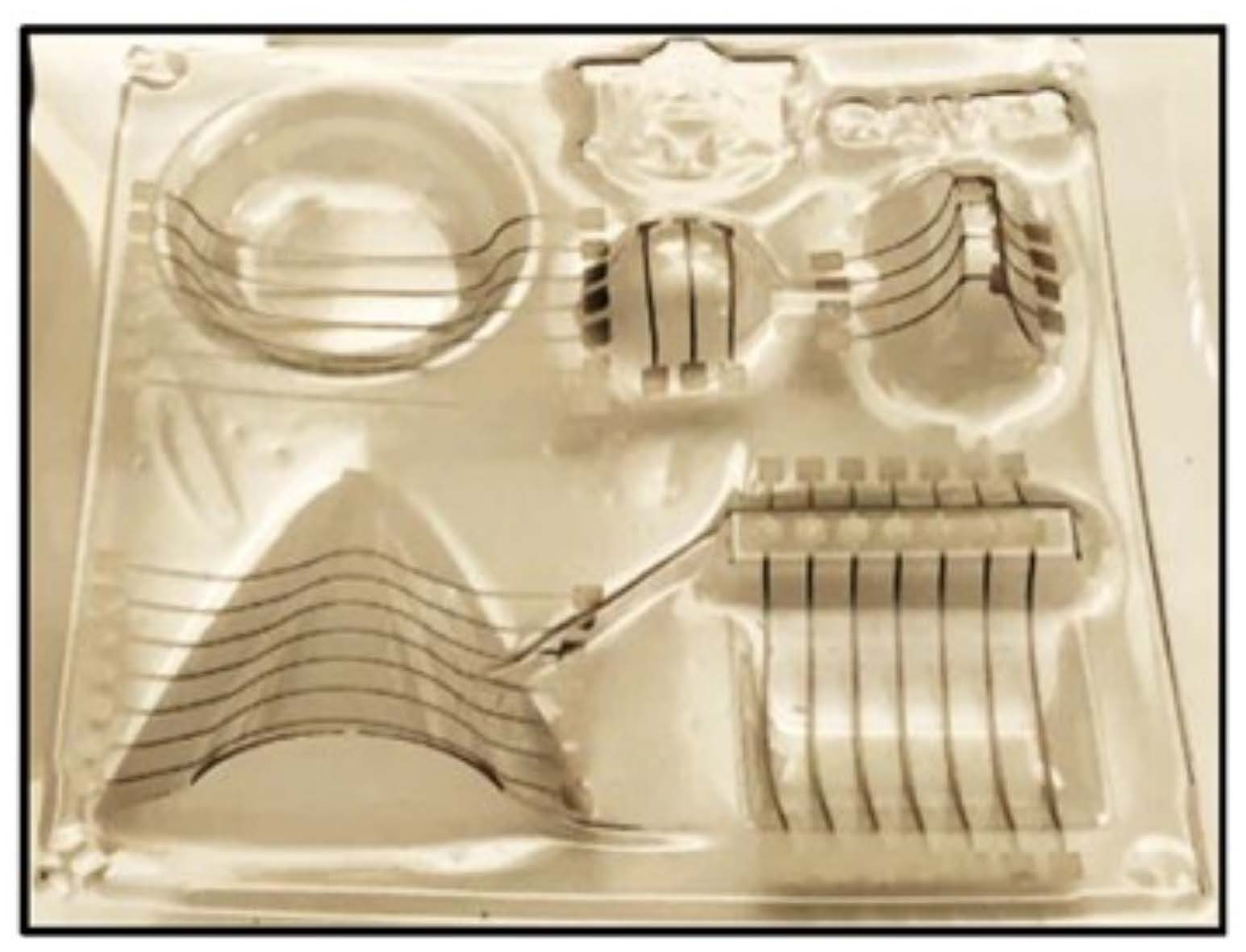
In the IME process, electronic circuits are printed onto a thin, flexible substrate, such as polyethylene terephthalate glycol (PETG) or polycarbonate (PC), which is then thermoformed using a mold. The thermoformed sample is then overmolded with another thermoplastic, resulting in a single, integrated part that combines the functionality of the electronic circuit with the mechanical properties of the plastic part. Using IMEs offers several benefits such as weight and bulk minimization, along with maintaining ergonomic design, which are important concerns in automotive design.
In this study, additively printed lines have been printed using the gravure offset printing technique on different substrates such as PETG and PC. These substrates have been subjected to vacuum thermoforming, wherein the substrates are heated to their heat deflection temperature and vacuum formed on an aluminum mold. The change in resistance of the lines pre- and post-thermoforming, as well as the effect of the degree of material stretching of the substrate with different thermoforming parameters such as thermoforming temperature and thermoforming time, has been studied. Finally, a component attachment study has been conducted for thermoformed circuits with a functional thermoformed full-wave rectifier circuit demonstrator.
REPAIRABILITY OF SMDS ON 3D PRINTED CIRCUITRY FOR SUSTAINABLE ELECTRONICS UTILIZING DIRECT WRITE TECHNIQUE
Sustainable conductive ink for 3D-printed flexible electronics is needed to enable lower-impact waste print processes. The ability to undertake reparability is an additional method to achieve sustainable products through the extension of electronic components’ lifespan and reduced e-waste. However, repairability studies are scarce for sustainable, flexible electronics in the literature. This study assessed the repairability potential of Surface Mount Devices (SMD) on 3D-printed full wave rectifier circuits for sustainable flexible electronics. Full wave rectifiers are commonly used in power supplies, battery chargers, and other applications requiring a steady DC voltage.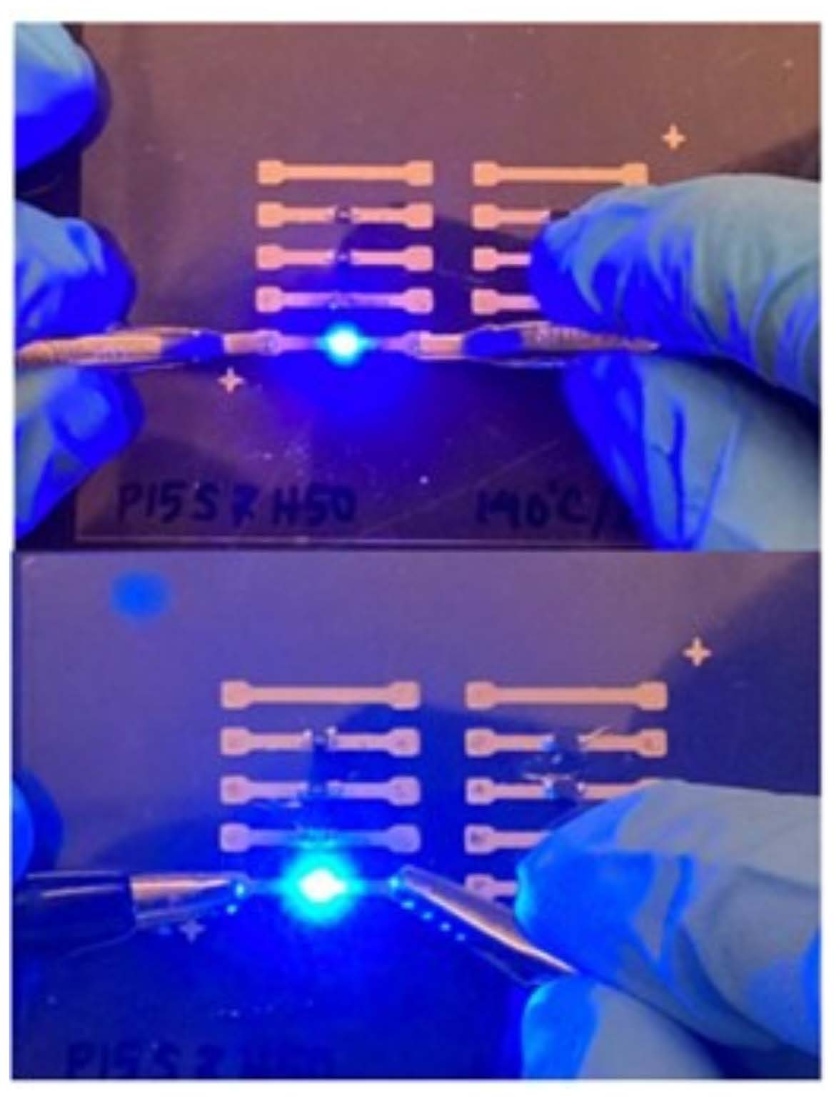
The direct-write printing technique used stretchable silver ink and interconnects composed of electrically conductive adhesive (ECA) for component attachment to create conductive traces. The circuit’s electrical characteristics are assessed using a high-frequency impedance analyzer, which analyzes the circuit’s resistance, capacitance, and inductance at various frequencies. The circuit is deliberately damaged by removing SMDs, and the research looks into the efficiency of direct-write repair procedures. Direct-write repair entails printing a conductive pad onto the circuit surface selectively using the same direct-write technique that was used for manufacturing the circuit. The repaired circuits are evaluated using an impedance analyzer, and the results are compared to the original circuit to determine the influence of the repair procedure on the circuit’s electrical performance.
DIRECT WRITE THERMOFORMED ADDITIVE SILVER CIRCUITS WITH SMDS ATTACHMENT FOR IN-MOLD ELECTRONICS
Additively printed thermoformable circuitry for In-Mold Electronics (IME) is gaining tremendous research focus because of its numerous advantages: design flexibility, cost-effectiveness, weight reduction, and potential for seamless integration into structural components. This study uses a direct write printing technique to produce conductive Full Wave Rectifier (FWR) circuits using stretchable silver ink. A stretchable ink capable of thermoforming was used for circuit fabrication. Once the conductive traces were printed, Surface Mount Devices (SMDs) were joined to the circuit using Electrically Conductive Adhesive (ECA). An impedance analyzer was used to examine the performance of the additively printed FWR circuit.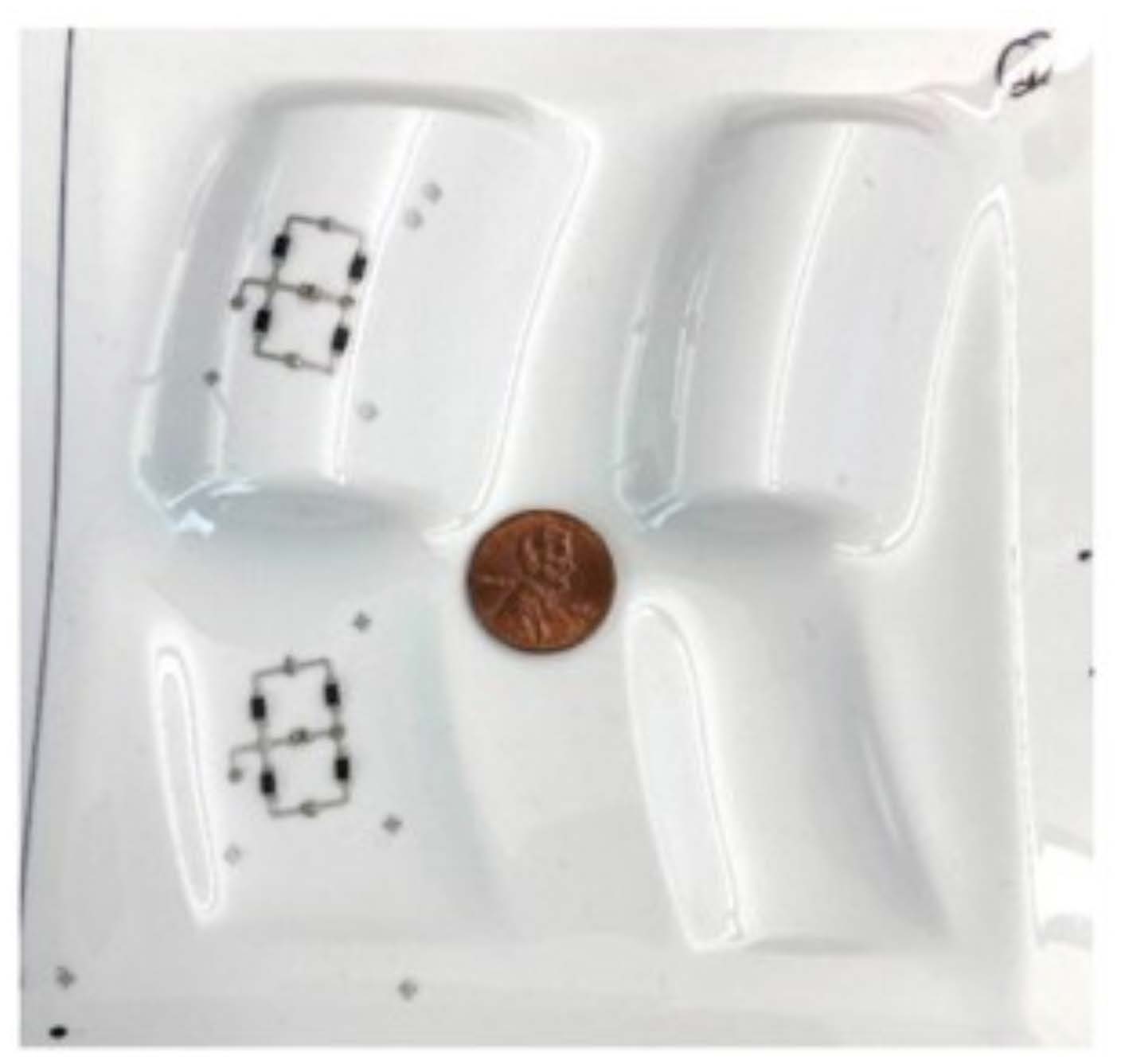
Thermoforming capable High Impact Polystyrene (HIPS) sheet and Polycarbonate (PC) substrates have been used for this study. The cross-section of the printed lines has been measured using white-light interferometry. The effect of the process parameters on the printed line resistivity has been studied. Optimized parameters from the printing process and sintering analysis are used to print FWR circuitry. The OrCAD software is used to simulate the FWR circuit. The simulated performance of the circuit is compared to the actual output of the printed thermoformed circuit.
COMPONENT ATTACH PROCESS RECIPE AND PERFORMANCE ON AEROSOL PRINTED SUSTAINABLE SILVER INK
The advancement of flexible printing technology in electronics has raised the demand for compact, lightweight, and stretchable printed electric circuits. The viability of environmentally friendly water-based inks with low-impact waste requires the development of process recipes for component attachment on flexible substrates. The processes required for component attachment on the newer generation of inks are not well understood.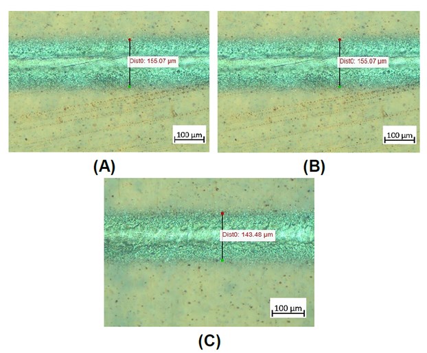
This paper aims to demonstrate a process parameter study and component attachment in the aerosol jet printer (AJP) platform with water-based silver nanoparticle ink. The process parameter study includes printing parameters such as UAMFC, SMFC, stage speed, number of passes, and sintering analysis, including sintering time and temperature. Print quality is evaluated using white light interferometry (WLI) and optical microscopy images. By integrating the bell-shaped cross-section area (CSA) acquired by the WLI test, the CSA of the printed lines is computed. The electrical and mechanical properties of the printed lines are quantified in terms of resistivity and shear load to failure, respectively.
Optimized parameters from the printing and sintering process are used to print traces on which different components are attached with the help of Electrically Conductive Adhesive (ECA). The effect of using sustainable ink and ECA on passive components was analyzed by comparing their performance before and after being attached. Components that fall within the acceptable range of the rated value are deemed to be functioning properly.
FUNCTIONAL CIRCUIT PERFORMANCE OF PRINTABLE FORMABLE INKS FOR IN-MOLD ELECTRONICS APPLICATIONS
In-mold electronics (IME) is an advanced technology that seamlessly integrates printed electronics with film insert molding, producing plastic components embedded with electronic functionalities. This innovative process combines printing, thermoforming, and injection molding, enabling the creation of intricate and tailored electronic devices. Its applications span various industries, including automotive components, household appliances, and consumer electronics, where bespoke user interfaces are essential for system management and monitoring. Customized interfaces play a pivotal role in automotive, industrial electronics, and consumer technology, encompassing features like knobs, pressure and toggle switches, analog instruments, and touch-sensitive flat-screen technology. IME's notable advantage lies in its capacity to fabricate flexible and stretchable electronic devices capable of functioning under strain, bending, stretching, and deformation.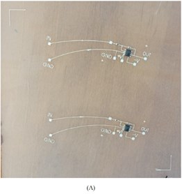
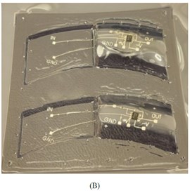
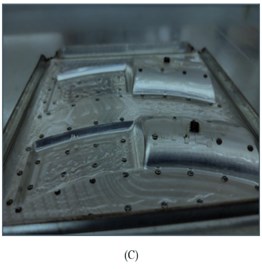
Despite its potential, the IME process encounters challenges, notably the electrical resistance fluctuations in printed circuits during thermoforming. This study addresses these challenges by introducing novel design strategies, incorporating electrically conductive adhesives (ECA) to affix components before thermoforming. This innovative approach preserves the integrity of the printed circuit, enhancing interconnect performance. To assess the IME process, the study employs OrCAD software for building and simulating a digital circuit, comparing its performance against the tolerance limits of Commercial Off-The-Shelf (COTS) components.
EFFECT OF THERMAL CYCLING ON INTERFACIAL FRACTURE TOUGHNESS OF ELECTRONIC MOLD COMPOUND-TO-SUBSTRATE INTERFACE SUBJECTED TO MONOTONIC AND FATIGUE LOADING
PREDICTION OF PAD CRATERING PERFORMANCE AT COPPER-RESIN INTERFACES WITH MULTIPLE REFLOWS
Pad cratering is one of the major failure modes encountered during PCB assembly and operation. Fracture is generally mechanically induced between the outermost layer of board resin and copper foil, between the resin and the glass fibers, or in the bulk resin of the printed circuit board. Prior work on the reliability of printed circuit board assemblies focuses on solder joint fatigue. However, data on the reliability of pad cratering and predictive models on expected pad-crater propensity are scarce.
Mechanical characteristics of the copper/resin interfaces and bulk resin material evolve with reflows. Pad cratering at copper-to-resin interfaces with respect to reflows has not been widely studied yet. In this study, ten distinct bulk resin materials have been investigated to compute the evolution of bulk resin properties. Copper-to-resin interfacial samples have been tested under four-point bend loading with respect to reflow conditions. The evolution of bulk resin properties has been considered for computing the evolution of copper/resin interfacial properties. The steady-state energy release rate and Interfacial Fracture Toughness are determined for each testing condition.
PREDICTION OF FAILURE AT FCBGA INTERFACES UNDER THERMO-MECHANICAL LOADS USING A COMPETING RISK COHESIVE ZONE MODEL
Automotive under-the-hood electronics may reside on-engine, on-transmission, or in-wheel-well. Several high I/O advanced packaging architectures, including flip-chip ball grid arrays (FCBGAs), enable much of the functionality. Underhood electronics in automobiles are an integral part of the critical and safety operations of the vehicle. Underfills significantly reduce the amount of plastic work during temperature excursions and offer mechanical support to the solder connections. One of the most common failure modes at chip/underfill (UF) interfaces has been delamination. A critical characteristic in evaluating the chip/UF interfacial reliability is the interfacial fracture toughness of the chip/UF interfaces. The interfacial crack could rapidly spread to the solder joints, leading to system failure. The chip/UF interface properties may change over time in response to high-temperature exposure.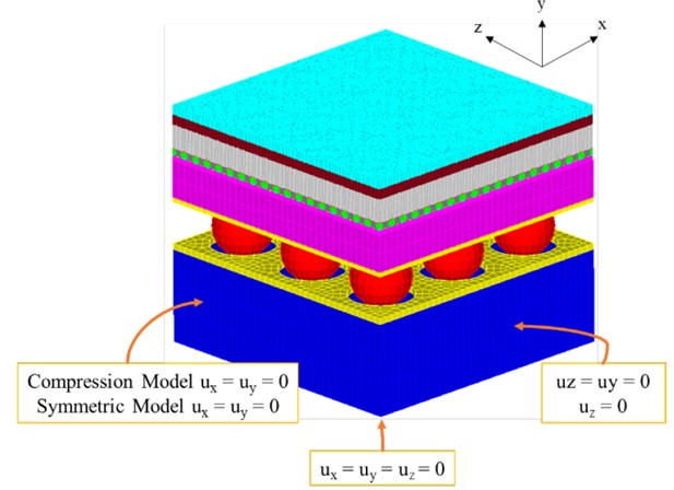
In this study, bi-material specimens of chip/UF interfaces have been fabricated and exposed to high temperatures of 100°C and 150°C for 30 days, 60 days, 90 days, 120 days, 180 days, 240 days, 300 days, and 360 days. The aged samples are subjected to four-point bend fatigue and monotonic loading. The interfacial fracture toughness values have been determined for each loading condition. The Paris constants (A, n) are computed from fatigue loading interfaces, which directly represent the evolution of interfacial properties with respect to sustained high temperature exposure. A predictive finite element model of the FCBGA interfaces has been created.
STUDY OF SUSTAINED HIGH-TEMPERATURE ON THE RELIABILITY OF LEAD-FREE SOLDER JOINT ASSEMBLIES UNDER VIBRATION
Electronic components in automotive, downhole drilling for oil & gas, and aerospace applications often face intense high-strain loads due to shocks, vibrations, and drop impacts. These components are also exposed to extreme temperatures ranging from -65°C to 200°C and experience strain rates of 1 to 100 per second in critical environments. SAC solder alloys, composed of tin, silver, and copper, are commonly used in place of tin-lead solders in electronic assembly applications. These lead-free alloys, such as SAC-Q, SAC-R, Innolot, and M758, are RoHS certified and safer than lead solder, which is neurotoxic. Understanding the mechanical characteristics of lead-free solder alloys is crucial for enhancing the durability of electronic packages under high temperatures and strain rates.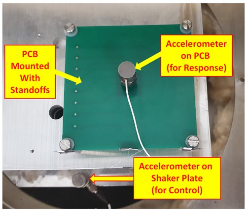
This study focuses on investigating SAC alloy failure mechanisms at elevated test temperatures up to 155°C and vibration loads of 5g and 10g levels. Harmonic vibrations at the first natural frequency were measured, and the assembly response and resistance were recorded using high-speed data acquisition and imaging. Finite Element Analysis (FEA) simulation was employed to calculate stresses in solder interconnects. The impact of g-levels and operating temperatures on the hysteresis loop and plastic work density was explored, and failure mode analysis was conducted on the test board. The study utilized previously published Anand viscoplasticity material data for the solder alloys to capture high-strain rate behavior and temperature-dependent aging in FEA.
EVOLUTION OF THERMAL INTERFACE MATERIAL-TO-COPPER INTERFACIAL FRACTURE TOUGHNESS SUBJECTEDTO MONOTONIC AND FATIGUE LOADING AFTER THERMAL CYCLING
Automotive electronics increasingly use high-performance semiconductors to enable a number of advanced driver assistance systems. Thermal management in chip-based electronic systems is quickly becoming one of the most significant impediments to enhanced performance and integration density. The ongoing downsizing and integration of semiconductor devices have increased the heat generated per unit volume of the chip. Thermal interface material (TIM) facilitates heat dissipation from the chip to the package and from the package to the heat sink. Exposure to the wide temperature ranges typical in automotive conditions may result in the early propagation of fractures at the TIM-to-Copper contact, leading to high thermal resistance and device thermal runaway.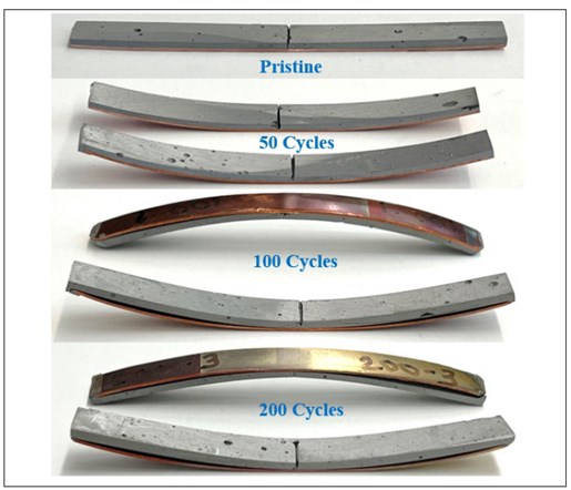
In this study, bi-material samples have been created by dispensing TIM materials onto the copper surface and curing them based on the specified conditions. A total of three different TIM materials are used in this study. Two types of samples are prepared, namely with and without pre-crack. The samples are tested in four-point bend monotonic and fatigue loading conditions. The pre-cracked samples are used for fatigue four-point bend loading, and the no pre-crack samples are used for monotonic four-point bend loading. Before testing, the bi-material samples are subjected to automotive-grade thermal cycling from -40°C to +125°C for up to 1000 cycles to calculate the KIC and KIIC fracture toughness values. Interfacial crack initiation, propagation, and failure mechanisms are investigated. The interface's strain energy release rate and fracture toughness are assessed.
ASSESSMENT OF PROPENSITY FOR PAD CRATERING AT THE BOARD RESIN-GLASS INTERFACE UNDER ASSEMBLY AND REWORK
Reliability requirements for harsh environment electronic packages are increasing with the use of electronics in automotive underhood applications. The underhood includes various safety and critical functions such as automated locking systems, electronic fuel injection systems, engine control units, and anti-lock braking systems. Pad cratering manifests with the initiation and propagation of micro-cracks beneath the BGA packages in the organic printed circuit boards. Major factors contributing to these cracks include a combination of thermal cycling, shocks, vibrations, incorrect design or material selection, and manufacturing defects.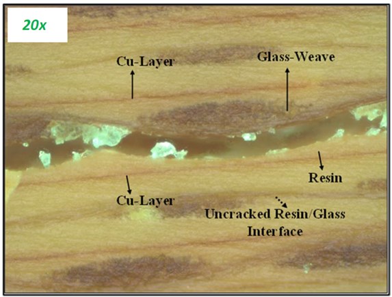
In this investigation, the problem of pad cratering has been systematically approached by analyzing the bulk behavior of the resins using a tensile dogbone specimen and then moving forward with a bent specimen for the glass-resin interfaces. The first bulk study consists of 12 different resin formulations in which material property changes were studied under two and six reflow cycles. In the second part, a four-point bend interface specimen was used. The effect of reflow cycles was investigated by reporting the percentage change in the Mode-I stress intensity factor and using this metric to rank the interfaces. In the end, an effort was made to create a predictive regression model with predictors being material properties of the samples such as elastic modulus, toughness, UTS, elongation of the resins, glass transition temperatures, and environmental conditions such as reflow cycles.
INCORPORATION OF DAMAGE IN CREEP MODELS FOR SAC305 LEAD FREE SOLDER
EVOLUTION IN LEAD-FREE SOLDER ALLOYS SUBJECTED TO BOTH MECHANICAL CYCLING AND AGING
Solder joints in electronic packaging frequently encounter failure from cyclic thermo-mechanical loading, especially in demanding environments like automotive engine compartments or industrial power plants. These components undergo both thermal cycling and mechanical cycling due to vibrations, along with thermal stresses from frequent power switching. As a result, the solder materials attaching these electronic components endure cyclic stresses and strains from temperature fluctuations, assembly material mismatches, and dynamic loadings.
Recent studies by our group have explored the mechanical behavior and property evolution of lead-free solder alloys due to either isothermal aging or isothermal mechanical cycling. Isothermal aging primarily induces microstructure changes, while mechanical cycling involves both microstructural evolution and damage accumulation, such as microcrack growth. However, no prior investigations have explored the combined effects of isothermal aging and mechanical cycling on the mechanical properties and microstructural evolution of lead-free solder alloys.
In this study, uniaxial samples of SAC305 lead-free solder alloy underwent solidification in glass tubes following a controlled reflow profile. The samples experienced mechanical cycling under strain control for various durations, followed by aging for 20 days at 125°C. Nanoindentation testing was then conducted to evaluate mechanical properties, revealing significant deteriorations, especially in samples cycled 300 times followed by aging. Optical microscopy confirmed microstructural coarsening due to the combined effects of mechanical cycling and aging. This research sheds light on the intricate interactions influencing the degradation of elastic modulus, hardness, and creep properties in solder alloys subjected to both aging and mechanical cycling.
PREDICTIVE MODELING OF HIGH-G POTTED ASSEMBLIES WITH FINE PITCH ELECTRONICS AFTER SUSTAINED HIGH-TEMPERATURE EXPOSURE
In the domains of defense and aerospace, electronic components endure intense G shock and thermo-mechanical loads, necessitating paramount reliability in these demanding environments. To enhance the dependability of printed circuit boards (PCBs) in such applications, potting is employed; however, interfacial delamination at the potting/PCB junction remains a predominant failure mode. Over time, the interfacial characteristics of this junction evolve due to prolonged exposure to elevated temperatures, prompting an investigation into the ramifications of such exposure on interface properties.
This study concentrates on scrutinizing the transformation of interfacial properties at the potting/PCB interface in response to high-temperature exposure and the implementation of restraint mechanisms.

A circular PCB featuring fine-pitch electronic packages and multilayer ceramic chip capacitors is assembled for experimentation. Bimaterial specimens of potting/PCB are fabricated, subjected to four-point bend loading, and examined to determine interfacial fracture toughness properties and cohesive zone parameters. Additionally, potted circular PCBs with various potting materials undergo testing for both pristine conditions and 90-day aging at 150°C. Shock levels of 10,000g and 25,000g are applied to assess the efficacy of potting compounds on the reliability of solder joints in fine-pitch electronics and large discrete components.
This investigation delves into a facet of potting electronics not previously explored, potentially influencing manufacturers. Validated cohesive zone parameters are utilized to devise a predictive finite element high G shock model for circular board assemblies. The experimental conditions are corroborated with the model's output, offering a comprehensive understanding of the potting/PCB interface's interfacial properties. The study also contemplates the prospective application of the predictive model in designing electronic components for harsh environments, providing valuable insights for manufacturers in this specialized field.
EFFECTS OF GRAIN TO SAMPLE VOLUME RATIO ON THE DEFORMATION BEHAVIOR OF POLYCRYSTAL SAC SAMPLES SUBJECTED TO SHEAR LOADS
As electronic components continuously shrink in size, understanding the size effects on the behavior of solder materials in electronic structural components becomes crucial. While extensive studies describe the deformation behavior of bulk SAC (Sn-Ag-Cu) alloys, the impact of size effects on solder deformation in small-scale joints is often overlooked. This study emphasizes the significance of obtaining a constitutive model that accounts for material behavior at smaller scales, particularly considering the increasing miniaturization of solder joints in high-density packaging.
SAC alloys, comprising more than 95% weight percentage of β-Sn, are extensively used for solder interconnects in microelectronic packaging. The anisotropic nature of β-Sn in terms of elastic modulus and coefficient of thermal expansion, along with its crystalline structure, influences plastic deformation through various atomic planes and slip systems. Crystal plasticity theory, implemented through a DAMASK code, is employed to elucidate the mesoscale deformation behavior of polycrystalline beta-tin samples. The study utilizes Voronoi tessellation to generate polycrystalline models with random grain orientations and explores shear simulations for different grain sizes.
The findings reveal that larger grain sizes exhibit isotropic deformation, while smaller grain sizes display anisotropic behavior under shear loads. This investigation sheds light on the critical grain size to sample size ratio where isotropic behavior transitions to anisotropic behavior during shear loading.
COMPARATIVE FINITE ELEMENT ANALYSES OF THE THERMAL CYCLING PERFORMANCES OF BGA PACKAGES WITH SAC, LTS, AND MIXED SAC-LTS SOLDER JOINTS
Understanding the mechanical behavior and reliability of lead-free microelectronic assemblies is crucial, especially for low-melting-point solders like Sn-Bi subjected to thermal cycling. While the industry often relies on the standard SAC (Sn-Ag-Cu) soldering alloy, the increasing use of Sn-Bi solder, with its lower reflow temperature and reduced warpage, emphasizes the need for mechanical characterization.
The 42%Sn-58%Bi solder (LTS) is commonly employed in mounting ball grid array (BGA) packages, creating mixed solder joints with SAC solder balls during reflow. Mechanical characterization of these mixed joints under various thermal cycling conditions is vital for predicting electronic package reliability. The study employs quarter-symmetry 3D models representing a plastic BGA package with eutectic Sn-Bi, mixed Sn-Bi/SAC305, and homogeneous SAC305 solder joints. Utilizing Anand parameter coefficients, the models simulate the nonlinear mechanical behaviors of both solders. Thermal cycling between -40 to 125°C is applied to predict thermal fatigue life (TFL) for each solder joint configuration under different PCB surface finishes.
The results indicate that the mixed Sn-Bi/SAC joint exhibits the highest TFL, followed by SAC305, and eutectic Sn-Bi (58Bi-42Sn) joints. Despite failure occurring at the top SMD end, significant plastic work accumulation at the SAC/SnBi interface suggests a nuanced failure mechanism. This study not only estimates TFL but also provides insights into the failure mechanisms of mixed LTS and SAC solder joint configurations under diverse thermal cycling conditions and PCB surface finishes.
SURFACE-MOUNT COMPONENT ATTACHMENT ON AEROSOL JET PRINTED SUSTAINABLE WATER-BASE SILVER NANOPARTICLE INK
Additive methods are preferred over processes that need hard tooling due to ramp-up speed and soft tooling. Increasing demand for the miniaturization of electronics has accelerated the development of flexible electronics technology. Flexible electronic architectures have gained traction in products for various end applications. The prior generation of additive processes used volatile organic solvent-based inks to fabricate printed circuits. Increased emphasis on environmental, social, and governmental factors has called attention to the development of sustainable products. Recent material development has seen the emergence of water-based inks with low-impact environmental waste. Sustainable inks use water as the carrier medium in place of volatile solvents. Owing to the recent introduction of these formulations, less is known about the ability to form functional circuits with sustainable inks or their performance relative to the incumbent non-sustainable volatile organic solvent-based inks.
In this paper, components were attached to additively printed water-based ink circuits fabricated using an aerosol jet. Interconnect methods have been studied, including electrically conductive adhesives. The component performance of RLC has been studied as a function of operating frequency and compared with the rated values. Mechanical performance has been studied using the shear load to failure and electron dispersive x-ray spectroscopy. The electrical performance has been correlated with the mechanical performance, and optical methods have also been used to characterize the results of the printed trace.
PROCESS PERFORMANCE INTERACTIONS FOR ADDITIVELY PRINTED WATER-BASED NAOPARTICLE SUSTAINABLE SILVER-INK WITH ULTRASONIC ATOMIZATION ON AEROSOL JET PRINTER
Environmental, social, and governmental factors have received increased attention in the design and manufacture of electronics. Additive printed electronics processes reduce the waste streams from electronics manufacturing by eliminating plate and etch processes, which involve the selective removal of masks and conductive copper to fabricate circuits. In addition, the transition to additive print processes also allows for the elimination of hard tooling, with design changes limited to those that can be implemented quickly, reducing the time involved with design iterations.
The earlier versions of additive inks involved using volatile solvents as carrier mediums for nanoparticle inks. Sustainable inks use water as the carrier medium in place of volatile solvents. Owing to the recent introduction of these formulations, less is known about the ability to form functional circuits with sustainable inks or their performance relative to the incumbent non-sustainable volatile organic solvent-based inks.
In this study, the performance of sustainable water-based solvent inks has been studied and compared with that of volatile solvent inks. The Aerosol Jet printer was used in this work to print and develop process parameters for investigation, including ultrasonic atomizer mass flow rate, sheath flow control, and stage speed, with a water-based sustainable silver nanoparticle ink. Electrical and mechanical properties were tested at various sintering temperatures and times, including resistance and shear load to failure. The results show that the electrical properties are improved by varying these parameters, and optical methods have also been used to characterize the results of the printed trace. Fitted regression models have been developed for process optimization.
INVESTIGATION OF PERFORMANCE AND REPAIRABILITY OF ADDITIVELY PRINTED FUNCTIONAL CIRCUITS WITH WATER-BASED SILVER INK ON AN INKJET PLATFORM
Additive printing techniques, particularly inkjet printing, have gained significant traction in the manufacturing of electronic circuits due to their cost-effective and time-efficient nature. Inkjet printing offers several advantages over traditional methods like screen printing, including the ability to print fine lines and utilize a broader range of conductive inks. Water-based silver ink is an environmentally friendly and highly conductive option. The water-based formulation eliminates the need for toxic solvents, ensuring a safer manufacturing and disposal process.
This research focuses on evaluating the performance of functional circuits additively printed with water-based silver ink using an inkjet platform. The circuits were printed onto a flexible polyimide substrate using an inkjet printer with a piezoelectric printhead. Functional circuits comprising High-Pass and Low-Pass Signal Filters were printed using water-based silver ink, with discrete commercial off-the-shelf (COTS) components attached. The frequency response of these circuits was measured and compared to simulated responses to determine any deviations in electrical performance.
The viability of repairing printed circuits was studied by intentionally detaching and reattaching the components. The repaired circuits were then compared to the pristine circuits in terms of their electrical performance.
DEVELOPMENT AND RELIABILITY EVALUATION OF ADDITIVELY PRINTED BIOSENSING DEVICE FOR WEARABLE APPLICATIONS IN HARSH ENVIRONMENT
Additive technologies have become increasingly favored for producing printed circuit boards (PCBs), eliminating the need for expensive tooling like photomasks or etching containers. The reliance on software-based design and manufacturing not only allows for greater production flexibility but also facilitates quicker tool adjustments and design developments. In contrast to traditional methods that involve subtracting unwanted material from a copper-clad board, additive printing methods can be applied to various fabrics, vehicles, and polymers with different surfaces and forms. This adaptability enables the creation of PCBs designed to fit diverse shapes and surfaces, fostering creativity and versatility in applications.
This flexibility extends to applications like wearable biosensors, incorporating an electrocardiography (ECG) sensor, electrodermal activity (EDA) sensor, pulse-oximetric sensor, body temperature sensor, and humidity sensor. These biosensors can monitor various aspects of human health, providing valuable data for medical diagnosis, fitness tracking, and stress management. Despite the potential of additively printed wearable biosensors, challenges related to reliability and durability exist, particularly when subjected to flexing forces and environmental conditions. Addressing stability concerns requires advancements in printing techniques, process recipes, and encapsulation materials.
In this research study, the direct-write (D-write) printing approach was employed to create an integrated wearable biosensor patch. The biosensor features circuits, encapsulations, a body temperature sensor, a humidity sensor, a pulse-oximetric sensor, and an electrodermal activity sensor. Electrically conductive adhesive (ECA) pads were also printed to attach components like a flexible battery, microcontroller, and wireless module. The developed firmware and data acquisition software allow the biosensor to collect and transmit biosignals to mobile devices. The biosensor underwent rigorous testing under varying conditions, demonstrating accuracy, repeatability, stability, sensitivity, linearity, response time, and hysteresis effects for each sensor.
The study contributes to the advancement of sustainable additive manufacturing for healthcare applications, showcasing a reliable and flexible integrated wearable biosensor.
ADDITIVE PRINTING OF WEARABLE EDA SENSORS ON INMOLD ELECTRONICS ON AUTOMOTIVE PLATFORM
Additive manufacturing techniques revolutionize the production of printed circuit boards (PCBs) by eliminating the need for expensive equipment like etching vessels and photomasks. Software-driven design not only ensures production flexibility but also facilitates rapid tool modifications and design enhancements. In contrast to traditional methods requiring complex processes, additive printing methods offer versatility by working on various substrates, vehicles, and polymers with diverse geometries and textures. This newfound flexibility sparks creativity among engineers, enabling the design of innovative applications such as wearable biosensors for monitoring diverse aspects of human health and stress, like the electrodermal activity (EDA) sensor. 
However, concerns arise regarding the stability of current wearable biosensor technology under flexural strain and harsh environmental conditions. To address these challenges, this research study introduces additive fabrication methods for creating PCBs for wearable biosensors without the need for costly equipment or intricate processes. Leveraging the benefits of software-driven design, the focus is on the EDA sensor, designed to measure skin conductance for driver monitoring. Using a direct-write printing technique with an nScrypt printer, the EDA sensor circuits are printed on thermoformable substrates. These substrates, moldable by heat and pressure, enable the PCBs to take various shapes for reliability testing.
The biosensor's performance is rigorously evaluated under different harsh conditions, including thermoformed shapes, temperature, humidity, and human body status, mirroring real-world driving scenarios. The results demonstrate that the additive PCB-based EDA sensor successfully measures skin conductance with acceptable error margins, showcasing mechanical robustness and reliability in diverse conditions. In conclusion, the developed EDA sensor utilizing additive fabrication techniques represents a milestone in monitoring driver stress levels with high reliability and flexibility.
COMPARATIVE STUDY OF SMD COMPONENTS ATTACHED USING ELECTRICALLY CONDUCTIVE ADHESIVE AND MAGNETICALLY ORIENTED ANISOTROPIC CONDUCTIVE ADHESIVE ON INKJET PRINTED STRUCTURES
Due to its high resolution and ability to deposit a variety of functional materials, including conductive inks, insulators, and dielectrics, inkjet printing is a viable method for constructing electronic devices. In this study, the authors sought to examine the electrical and mechanical performance of surface-mounted device (SMD) components mounted on inkjet-printed circuits using two adhesives: Electrically Conductive Adhesive (ECA) and Magnetically Oriented Anisotropic Conductive Adhesive (MOACA). 
The study is carried out in two phases. In the initial phase, SMD components such as resistors, inductors, and capacitors were mounted using ECA and MOACA on conductive traces with pads, and their electrical performance was compared to their rated values. In the second phase, the behavior of inkjet-printed circuits was studied, including Non-Inverting Amplifier Circuits and Schmitt Trigger Circuits. These functional circuits were constructed on polyimide substrates using silver nanoparticle ink.
Evaluation of the electrical and mechanical performance of the circuits was conducted. Overall, this study provides invaluable insight into the electrical and mechanical behavior of inkjet-printed circuits, particularly in the context of attached components.
LINE WIDTH AND ELECTRICAL PERFORMANCE PREDICTION FOR INKJET PRINTED CONDUCTORS-RESISTORS-INDUCTORS-CAPACITORS
Inkjet printing enables the high-speed production of devices on a variety of substrates while offering an increased level of precision and repeatability. There is a need for closed-loop control over the printing process to achieve geometrical accuracy and consistent electrical performance of printed circuits and components. A sophisticated closed-loop control process can be achieved by establishing a relationship between printer input parameters and the geometrical and electrical outputs of printed objects.
In this study, the impact of various printer settings on the electrical performance and geometrical accuracy of printed circuits and components was examined. Specifically, the effects of print resolution, droplet size, and the number of copies on the electrical performance of printed resistors, planar inductors, and capacitors were investigated. The printing was done using particle-free silver ink on a polyimide substrate.
The statistical model developed from experimental data provides a means of achieving closed-loop control over the printing process, ensuring consistent and accurate production of printed electronic components.
REPARABILITY TEST OF AEROSOL-JET PRINTED SUSTAINABLE SILVER INK CIRCUIT
The earlier generation of additive printable inks was based on volatile organic solvent carrier fluids. Increased awareness of the environmental impact of electronic waste has resulted in the emergence of environmentally friendly water-based inks with low-impact waste. The repairability of additively printed circuits can be used to reduce electronic waste and enable life extensions of deployed electronics through repair and replacement. However, the repairability potential, processes, and impact on reliability are relatively unexplored for new sustainable materials.
This study consists of a thorough examination of component attachment and the reparability of components on performance and reliability. Repair procedures have been pursued on circuits printed with sustainable conductive ink using an aerosol jet printer (AJP). Adhesives are printed on the pads at the location where the component is to be attached using a direct-write technique capable of printing highly viscous materials such as electrically conductive adhesive (ECA).
The procedure entails attaching a component to a flexible printed circuit, measuring the output response, removing the attached component from the circuit, replacing it with a new component of the same rated value, measuring the output again, and comparing it to the prior output and the simulated output. Furthermore, the mechanical strength of the attached components is characterized in terms of shear load to failure. The force required to remove the attached component using a metal tip before and after the repair is compared for each of the passive components. Finally, a functional differentiator circuit is used to validate the findings.
SUSTAINABLE SILVER INK FLEXIBLE CIRCUITS FABRICATION USING DIRECT WRITE ADDITIVE MANUFACTURING TECHNIQUES
Conventional inorganic inks used to fabricate additive circuits pose a significant environmental challenge due to their toxic nature and non-biodegradable properties. There is a need for a more sustainable alternative for the realization of additively printed electronics. Water-based inks, made from renewable and biodegradable materials, have emerged as a promising solution. 
This study focuses on examining process performance interactions for direct-write printed circuits and the attachment of surface-mount components. The authors investigate the ability of direct-write methods to create functional circuits while also exploring the effects of process parameters on the manufactured properties. Process recipes have been developed using a water-based sustainable silver ink applied to two different substrates (PET and Polyimide), and the impact of varying print parameters was compared among the substrates.
The findings reveal the influence of print parameters on the mechanical and electrical properties of the printed traces, as well as demonstrate the additive printing of circuits and the attachment of surface-mount components using the optimal process parameters. Furthermore, the performance of a printed Active Lowpass Filter was evaluated using LTspice software. This research aims to demonstrate the viability of direct-write technology as a sustainable and viable alternative for the manufacture of traditional electronic circuits by successfully attaching surface-mount components to printed pads.
IMPACT OF COMPONENT INTERCONNECTIVITY ON MECHANICAL AND ELECTRICAL PROPERTIES OF FLEXIBLE HYBRID ELECTRONICS WITH PRINTED WATER-BASED SILVER INK CIRCUITS
Flexible Hybrid Electronics (FHE) have the potential to revolutionize the electronics industry by providing sustainable and efficient devices. However, the reliable interconnectivity between printed traces and surface-mount devices (SMD) remains a critical challenge for FHE. There is a need for more research on the use of printed water-based silver ink traces and bonding materials for component attachment in FHE, as the literature on this subject is limited.
This study was conducted to compare the effects of different bonding materials on component attachment. The bonding materials investigated were electrically conductive adhesive (ECA) and low-temperature solder (LTS). The study used the direct write method to print silver pads, which were then used to attach components such as resistors, inductors, and capacitors using the bonding materials. Electrically conductive adhesive (ECA) results were compared to those of low-temperature solder (LTS).
The interconnectivity of the attached components was evaluated by measuring their rating values before and after attachment. The findings of this study provide insights into the performance of different bonding materials for component attachment in FHE. Such insights can aid in the development of reliable and efficient interconnectivity methods for FHE, which can contribute to the widespread adoption of FHE in various industries.
EFFECT OF SURFACE TREATMENT ON THE FATIGUE CRACK PROPAGATION IN A TIM/COPPER INTERFACE SUBJECTED TO HIGH-TEMPERATURE LONG-TERM EXPOSURE
As electronic devices continue to shrink, effective heat dissipation becomes a critical concern, impacting device reliability. When solid surfaces come into contact, the limited contact area, often only 1% to 2%, results in elevated contact resistance, approximately 100mm²/kW, between bare silicon-to-silicon contacts. To address this issue, thermal interface materials (TIMs) are employed to reduce contact resistance and enhance heat dissipation. Microelectronic packages incorporate multiple bi-material interfaces, influencing device design and reliability.
Dynamic mechanical analysis, such as a 4-point bending test, enables the study of fatigue failure in bi-layer materials. Cyclic loading stress is applied to characterize material fatigue and failure, allowing control over both strain and stress. As semiconductor devices increasingly operate at higher temperatures, reaching 125 – 200°C in high-power density electronics, there is a need for understanding how electronic components endure prolonged exposure to such conditions.
This study assesses the reliability and stability of grounded lid Flip-Chip Ball Grid Array (FCBGA) packages under high-temperature environments. It investigates the low cycle fatigue properties of TIM and copper bi-material interfaces, examining adhesion strength, fracture toughness, and stress intensity factors. The impact of aging time, plasma cleaning power, aging temperatures, and mode-mixity on fatigue crack propagation is explored through the application of Digital Image Correlation (DIC) technology. Paris’ law coefficients and exponents are found to be dependent on mode-mixity, indicating that certain fatigue properties can be derived from monotonic fracture behavior in bi-material interfaces.
COMPARISON OF MACHINE LEARNING APPROACHES FOR CORRELATING PRINT PROCESS PARAMETERS TO REALIZED PHYSICAL AND ELECTRICAL CHARACTERISTICS OF PRINTED ELECTRONICS USING INKJET PLATFORM
In the last decade, printed electronics has gained significant research attention, making inroads into consumer electronics. The key advantage of additive printed electronics lies in its ability to produce lightweight and flexible components at a lower cost than traditional methods. Various printing techniques, conductive inks, dielectrics, solder pastes, and electrically conductive adhesives have been explored to find optimal solutions. However, a common challenge is the disparity between designed and actualized geometrical and electrical characteristics of printed traces, affecting overall circuit performance.
This study focuses on developing a closed-loop control process for adjusting process parameters to achieve desired electrical and physical trace characteristics. Using an inkjet printer and particle-free silver ink, the study establishes a relationship between process parameters and line geometry. Different machine learning methods, including nonlinear regression and Gaussian process regression, are employed and optimized to create a graphical user interface (GUI) for a closed-loop control algorithm. This algorithm provides corrective print parameters based on desired, realized, and current parameters.
EVALUATION OF ADDITIVE CIRCUITS PRINTED WITH SUSTAINABLE AQUEOUS SILVER INKS USING AEROSOL JET PRINTING AND GRAVURE OFFSET PRINTING AND INVESTIGATION OF CIRCUIT REPAIRABILITY
Additive printed electronics, in particular, has been a rapidly advancing field, with applications that span from smart packaging to energy harvesting systems to healthcare devices to intelligent textiles. The basic building block of any flexible circuit created by these technologies is conductive ink. This ink typically comprises metal nanoparticles and several solvents. However, many of the solvents used in these inks are toxic substances or include volatile organic compounds (VOCs) that have a variety of negative effects on the environment and human health, including air pollution, smog, respiratory problems, health risks, and reduced air quality. Consequently, there is a strong push toward developing sustainable materials for use in products, including ink formulations with fewer toxic solvents.
In this study, researchers investigate the use of two printing techniques, aerosol jet printing and gravure offset printing, to print full-wave rectifiers (AC to DC conversion) and voltage bridge oscillators (DC to AC conversion) using commercially available aqueous silver ink. The performance of the additively printed circuits is compared to both theoretical values and to the same circuits printed using non-aqueous inks. Additionally, a switch-mode battery charging circuit has also been printed with a sustainable ink, and its performance has been investigated.
POLARIZATION CURVES, PACKAGE-LEVEL MULTIPHYSICS SIMULATION OF CU85AL15 AND CU94AL6 WB CORROSION FOR AUTOMOTIVE AND RUGGED ENVIRONMENT APPLICATIONS
EVALUATION OF THERMOFORMABILITY OF ADDITIVELY PRINTED CIRCUITS PRINTED USING GRAVURE OFFSET PRINTING TECHNIQUE AND INVESTIGATION OF IN-MOLD ELECTRONIC CIRCUITS
Throughout the past decade, the field of printed electronics has gained increased research impetus and has started to make entryways into the consumer electronics product market. The applications of additive printed electronics are numerous and range from healthcare devices and smart packaging to energy harvesting systems and intelligent textiles. Another novel application area for printed electronics is in-mold electronics (IME), which involves integrating printed electronic circuits into injection-molded parts.
In the IME process, electronic circuits are printed onto a thin, flexible substrate, such as polyethylene terephthalate glycol (PETG) or polycarbonate (PC), which is then thermoformed using a mold. The thermoformed sample is then overmolded with another thermoplastic, resulting in a single, integrated part that combines the functionality of the electronic circuit with the mechanical properties of the plastic part. Using IMEs offers several benefits such as weight and bulk minimization, along with maintaining ergonomic design, which are important concerns in automotive design.
In this study, additively printed lines have been printed using the gravure offset printing technique on different substrates such as PETG and PC. These substrates have been subjected to vacuum thermoforming, wherein the substrates are heated to their heat deflection temperature and vacuum formed on an aluminum mold. The change in resistance of the lines pre- and post-thermoforming, as well as the effect of the degree of material stretching of the substrate with different thermoforming parameters such as thermoforming temperature and thermoforming time, has been studied. Finally, a component attachment study has been conducted for thermoformed circuits with a functional thermoformed full-wave rectifier circuit demonstrator.
REPAIRABILITY OF SMDS ON 3D PRINTED CIRCUITRY FOR SUSTAINABLE ELECTRONICS UTILIZING DIRECT WRITE TECHNIQUE
Sustainable conductive ink for 3D-printed flexible electronics is needed to enable lower-impact waste print processes. The ability to undertake reparability is an additional method to achieve sustainable products through the extension of electronic components’ lifespan and reduced e-waste. However, repairability studies are scarce for sustainable, flexible electronics in the literature. This study assessed the repairability potential of Surface Mount Devices (SMD) on 3D-printed full wave rectifier circuits for sustainable flexible electronics. Full wave rectifiers are commonly used in power supplies, battery chargers, and other applications requiring a steady DC voltage.
The direct-write printing technique used stretchable silver ink and interconnects composed of electrically conductive adhesive (ECA) for component attachment to create conductive traces. The circuit’s electrical characteristics are assessed using a high-frequency impedance analyzer, which analyzes the circuit’s resistance, capacitance, and inductance at various frequencies. The circuit is deliberately damaged by removing SMDs, and the research looks into the efficiency of direct-write repair procedures. Direct-write repair entails printing a conductive pad onto the circuit surface selectively using the same direct-write technique that was used for manufacturing the circuit. The repaired circuits are evaluated using an impedance analyzer, and the results are compared to the original circuit to determine the influence of the repair procedure on the circuit’s electrical performance.
DIRECT WRITE THERMOFORMED ADDITIVE SILVER CIRCUITS WITH SMDS ATTACHMENT FOR IN-MOLD ELECTRONICS
Additively printed thermoformable circuitry for In-Mold Electronics (IME) is gaining tremendous research focus because of its numerous advantages: design flexibility, cost-effectiveness, weight reduction, and potential for seamless integration into structural components. This study uses a direct write printing technique to produce conductive Full Wave Rectifier (FWR) circuits using stretchable silver ink. A stretchable ink capable of thermoforming was used for circuit fabrication. Once the conductive traces were printed, Surface Mount Devices (SMDs) were joined to the circuit using Electrically Conductive Adhesive (ECA). An impedance analyzer was used to examine the performance of the additively printed FWR circuit.
Thermoforming capable High Impact Polystyrene (HIPS) sheet and Polycarbonate (PC) substrates have been used for this study. The cross-section of the printed lines has been measured using white-light interferometry. The effect of the process parameters on the printed line resistivity has been studied. Optimized parameters from the printing process and sintering analysis are used to print FWR circuitry. The OrCAD software is used to simulate the FWR circuit. The simulated performance of the circuit is compared to the actual output of the printed thermoformed circuit.
COMPONENT ATTACH PROCESS RECIPE AND PERFORMANCE ON AEROSOL PRINTED SUSTAINABLE SILVER INK
The advancement of flexible printing technology in electronics has raised the demand for compact, lightweight, and stretchable printed electric circuits. The viability of environmentally friendly water-based inks with low-impact waste requires the development of process recipes for component attachment on flexible substrates. The processes required for component attachment on the newer generation of inks are not well understood.
This paper aims to demonstrate a process parameter study and component attachment in the aerosol jet printer (AJP) platform with water-based silver nanoparticle ink. The process parameter study includes printing parameters such as UAMFC, SMFC, stage speed, number of passes, and sintering analysis, including sintering time and temperature. Print quality is evaluated using white light interferometry (WLI) and optical microscopy images. By integrating the bell-shaped cross-section area (CSA) acquired by the WLI test, the CSA of the printed lines is computed. The electrical and mechanical properties of the printed lines are quantified in terms of resistivity and shear load to failure, respectively.
Optimized parameters from the printing and sintering process are used to print traces on which different components are attached with the help of Electrically Conductive Adhesive (ECA). The effect of using sustainable ink and ECA on passive components was analyzed by comparing their performance before and after being attached. Components that fall within the acceptable range of the rated value are deemed to be functioning properly.
FUNCTIONAL CIRCUIT PERFORMANCE OF PRINTABLE FORMABLE INKS FOR IN-MOLD ELECTRONICS APPLICATIONS
In-mold electronics (IME) is an advanced technology that seamlessly integrates printed electronics with film insert molding, producing plastic components embedded with electronic functionalities. This innovative process combines printing, thermoforming, and injection molding, enabling the creation of intricate and tailored electronic devices. Its applications span various industries, including automotive components, household appliances, and consumer electronics, where bespoke user interfaces are essential for system management and monitoring. Customized interfaces play a pivotal role in automotive, industrial electronics, and consumer technology, encompassing features like knobs, pressure and toggle switches, analog instruments, and touch-sensitive flat-screen technology. IME's notable advantage lies in its capacity to fabricate flexible and stretchable electronic devices capable of functioning under strain, bending, stretching, and deformation.


Despite its potential, the IME process encounters challenges, notably the electrical resistance fluctuations in printed circuits during thermoforming. This study addresses these challenges by introducing novel design strategies, incorporating electrically conductive adhesives (ECA) to affix components before thermoforming. This innovative approach preserves the integrity of the printed circuit, enhancing interconnect performance. To assess the IME process, the study employs OrCAD software for building and simulating a digital circuit, comparing its performance against the tolerance limits of Commercial Off-The-Shelf (COTS) components.
EFFECT OF THERMAL CYCLING ON INTERFACIAL FRACTURE TOUGHNESS OF ELECTRONIC MOLD COMPOUND-TO-SUBSTRATE INTERFACE SUBJECTED TO MONOTONIC AND FATIGUE LOADING
PREDICTION OF PAD CRATERING PERFORMANCE AT COPPER-RESIN INTERFACES WITH MULTIPLE REFLOWS
Pad cratering is one of the major failure modes encountered during PCB assembly and operation. Fracture is generally mechanically induced between the outermost layer of board resin and copper foil, between the resin and the glass fibers, or in the bulk resin of the printed circuit board. Prior work on the reliability of printed circuit board assemblies focuses on solder joint fatigue. However, data on the reliability of pad cratering and predictive models on expected pad-crater propensity are scarce.
Mechanical characteristics of the copper/resin interfaces and bulk resin material evolve with reflows. Pad cratering at copper-to-resin interfaces with respect to reflows has not been widely studied yet. In this study, ten distinct bulk resin materials have been investigated to compute the evolution of bulk resin properties. Copper-to-resin interfacial samples have been tested under four-point bend loading with respect to reflow conditions. The evolution of bulk resin properties has been considered for computing the evolution of copper/resin interfacial properties. The steady-state energy release rate and Interfacial Fracture Toughness are determined for each testing condition.
PREDICTION OF FAILURE AT FCBGA INTERFACES UNDER THERMO-MECHANICAL LOADS USING A COMPETING RISK COHESIVE ZONE MODEL
Automotive under-the-hood electronics may reside on-engine, on-transmission, or in-wheel-well. Several high I/O advanced packaging architectures, including flip-chip ball grid arrays (FCBGAs), enable much of the functionality. Underhood electronics in automobiles are an integral part of the critical and safety operations of the vehicle. Underfills significantly reduce the amount of plastic work during temperature excursions and offer mechanical support to the solder connections. One of the most common failure modes at chip/underfill (UF) interfaces has been delamination. A critical characteristic in evaluating the chip/UF interfacial reliability is the interfacial fracture toughness of the chip/UF interfaces. The interfacial crack could rapidly spread to the solder joints, leading to system failure. The chip/UF interface properties may change over time in response to high-temperature exposure.
In this study, bi-material specimens of chip/UF interfaces have been fabricated and exposed to high temperatures of 100°C and 150°C for 30 days, 60 days, 90 days, 120 days, 180 days, 240 days, 300 days, and 360 days. The aged samples are subjected to four-point bend fatigue and monotonic loading. The interfacial fracture toughness values have been determined for each loading condition. The Paris constants (A, n) are computed from fatigue loading interfaces, which directly represent the evolution of interfacial properties with respect to sustained high temperature exposure. A predictive finite element model of the FCBGA interfaces has been created.
STUDY OF SUSTAINED HIGH-TEMPERATURE ON THE RELIABILITY OF LEAD-FREE SOLDER JOINT ASSEMBLIES UNDER VIBRATION
Electronic components in automotive, downhole drilling for oil & gas, and aerospace applications often face intense high-strain loads due to shocks, vibrations, and drop impacts. These components are also exposed to extreme temperatures ranging from -65°C to 200°C and experience strain rates of 1 to 100 per second in critical environments. SAC solder alloys, composed of tin, silver, and copper, are commonly used in place of tin-lead solders in electronic assembly applications. These lead-free alloys, such as SAC-Q, SAC-R, Innolot, and M758, are RoHS certified and safer than lead solder, which is neurotoxic. Understanding the mechanical characteristics of lead-free solder alloys is crucial for enhancing the durability of electronic packages under high temperatures and strain rates.
This study focuses on investigating SAC alloy failure mechanisms at elevated test temperatures up to 155°C and vibration loads of 5g and 10g levels. Harmonic vibrations at the first natural frequency were measured, and the assembly response and resistance were recorded using high-speed data acquisition and imaging. Finite Element Analysis (FEA) simulation was employed to calculate stresses in solder interconnects. The impact of g-levels and operating temperatures on the hysteresis loop and plastic work density was explored, and failure mode analysis was conducted on the test board. The study utilized previously published Anand viscoplasticity material data for the solder alloys to capture high-strain rate behavior and temperature-dependent aging in FEA.
EVOLUTION OF THERMAL INTERFACE MATERIAL-TO-COPPER INTERFACIAL FRACTURE TOUGHNESS SUBJECTEDTO MONOTONIC AND FATIGUE LOADING AFTER THERMAL CYCLING
Automotive electronics increasingly use high-performance semiconductors to enable a number of advanced driver assistance systems. Thermal management in chip-based electronic systems is quickly becoming one of the most significant impediments to enhanced performance and integration density. The ongoing downsizing and integration of semiconductor devices have increased the heat generated per unit volume of the chip. Thermal interface material (TIM) facilitates heat dissipation from the chip to the package and from the package to the heat sink. Exposure to the wide temperature ranges typical in automotive conditions may result in the early propagation of fractures at the TIM-to-Copper contact, leading to high thermal resistance and device thermal runaway.
In this study, bi-material samples have been created by dispensing TIM materials onto the copper surface and curing them based on the specified conditions. A total of three different TIM materials are used in this study. Two types of samples are prepared, namely with and without pre-crack. The samples are tested in four-point bend monotonic and fatigue loading conditions. The pre-cracked samples are used for fatigue four-point bend loading, and the no pre-crack samples are used for monotonic four-point bend loading. Before testing, the bi-material samples are subjected to automotive-grade thermal cycling from -40°C to +125°C for up to 1000 cycles to calculate the KIC and KIIC fracture toughness values. Interfacial crack initiation, propagation, and failure mechanisms are investigated. The interface's strain energy release rate and fracture toughness are assessed.
ASSESSMENT OF PROPENSITY FOR PAD CRATERING AT THE BOARD RESIN-GLASS INTERFACE UNDER ASSEMBLY AND REWORK
Reliability requirements for harsh environment electronic packages are increasing with the use of electronics in automotive underhood applications. The underhood includes various safety and critical functions such as automated locking systems, electronic fuel injection systems, engine control units, and anti-lock braking systems. Pad cratering manifests with the initiation and propagation of micro-cracks beneath the BGA packages in the organic printed circuit boards. Major factors contributing to these cracks include a combination of thermal cycling, shocks, vibrations, incorrect design or material selection, and manufacturing defects.
In this investigation, the problem of pad cratering has been systematically approached by analyzing the bulk behavior of the resins using a tensile dogbone specimen and then moving forward with a bent specimen for the glass-resin interfaces. The first bulk study consists of 12 different resin formulations in which material property changes were studied under two and six reflow cycles. In the second part, a four-point bend interface specimen was used. The effect of reflow cycles was investigated by reporting the percentage change in the Mode-I stress intensity factor and using this metric to rank the interfaces. In the end, an effort was made to create a predictive regression model with predictors being material properties of the samples such as elastic modulus, toughness, UTS, elongation of the resins, glass transition temperatures, and environmental conditions such as reflow cycles.


