7. MOSFETs and CMOS Inverter
7.1. Goal
Measure threshold voltage and Ids-Vgs in forced saturation configuration.
Measure the Ids-Vds curves for a multiple Vgs values.
An understanding of MOSFET switching circuits.
Build a CMOS inverter.
Experiment with overlocking and underclocking a CMOS circuit
More experience with the ELVIS II, Labview and the oscilloscope
Continue to develop professional lab skills and written communication skills.
7.2. Required Components
7.3. Required Soft Front Panels (SFPs)
2-wire I-V analyzer
FGEN
Scope
DMM
Digital Writer
7.4. Overview
A thorough treatment of MOSFETs can be found in Chapter 4 of the ELEC 2210 textbook, Microelectronics Circuit Design by R.C. Jaeger.
7.4.1. Transistor Characteristics
In this lab, we will first measure the I-V characteristics of MOSFETs, including:
Ids-Vgs in a saturation by connection configuration, e.g. with gate tied to the drain, from which we can determine threshold voltage.
Ids-Vds curves for multiple gate-to-source voltages (Vgs), from which we can observe linear and saturation operation regions.
Using measured threshold voltage and Ids-Vds curves, we can then check how well first-order MOSFET theory holds up in real devices and get a practical feel of the limitation of first-order theoretical MOSFET equation.
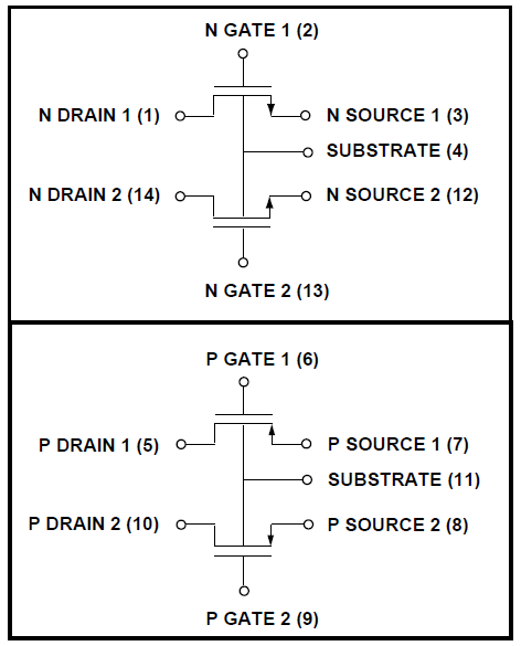
The MOSFETs we will use in this experiment are from ALD1105, an IC containing two n-MOSFETs and two p-MOSFETs. A circuit symbol description of the two pairs of transistors from the data sheet is shown below in figure 1.

Figure 1: Circuit Symbol and Pin Numbers for the Pairs of N-channel and P-channel MOSFETs.
Note each transistor has four terminals: drain (D), source (S), gate (G), and substrate, which is called body (B) in our text. As we learned in class, all the n-MOSFETs on an IC share the same p-type body, which needs to be tied to the lowest voltage in a system to keep all the source/drain to body PN junctions zero or reverse biased.
Similarly, all the p-MOSFETs on an IC share the same n-type body, which needs to be tied to the highest voltage in a system to keep all the source/drain to body PN junctions zero or reverse biased.
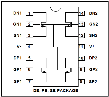
The pin diagram seen in figure 2 shows the package layout and various pin connections for ALD1105.

Figure 2: Pin diagram of ALD1105 package.
7.4.2. CMOS Inverter
MOSFETs are mostly used in CMOS circuits. There are many advantages of CMOS, with the biggest being zero standby power consumption, at least ideally.
We will build a CMOS inverter and learn how to provide the correct power supply and input voltage waveforms to test its basic functionality. For a given supply VDD, your voltage low should be zero, and voltage high should be VDD.
By default, the function generator gives an output that varies from -VPP/2 to +VPP/2, with VPP being peak-to-peak voltage. For a square wave, the voltage low is -VPP/2, voltage high is +VPP/2. You can set the DC offset to VPP/2 to make voltage low 0.
We will build complex CMOS logic gates and sequential CMOS circuits from scratch using transistors in other labs.
7.5. Pre-Lab
Using the
datasheet, determine the values of the threshold voltage range, the maximum continuous drain current ID, the maximum drain-source voltage, and the maximum allowed power dissipation, Ptot.In which region should the MOSFET be operating when it is a closed switch? Why? In which region should it be operating when it is an open switch? Why?
Draw a pin-level wiring diagram of a CMOS inverter. Use the pair of NMOS and PMOS gates on the right side of the ALD1105 IC.
For a VDD of 3V, 5V, 7V, sketch the input waveforms required to test the functionality of the CMOS inverter. Determine the VPP and dc offset setting required for function generator. Use square wave.
7.6. Lab Exercise
There are 6 parts and a bonus. Have your GTA sign off on each part before proceeding to the next part.
7.6.1. Ids-Vds and Ids-Vgs Using Custom Labview Program for NMOS
7.6.1.1. NMOS Ids-Vds Characteristics
To automate the measurement, we desire to have a curve tracer program like the 3-wire analyzer SFP that came with ELVIS II we had used earlier to measure bipolar transistors.
Unfortunately, that 3-wire curve tracer SFP is designed to work with bipolar transistors only. To make your lab easier, I have written a customized MOSFET curve tracer program.
Proceed as follows:
Make sure the ELVIS II power is turned off.
Make the connections to an rc4558 op-amp as shown in figure 3.

Figure 3: Circuit connections for NMOS Id-Vgs and Id-Vds measurements. Notice that there are two chips here RC4558(Opamp) and ALD1105 (NMOS).
Connect AO1 to the ALD1105 NMOS gate (pin 2), connect the current meter common terminal to the NMOS drain (pin 1), and connect the NMOS source and body (pins 3 and 4) to ground as shown in figure 3.
Open the LabVIEW program provided
here.Use the following settings:
Vgs start = 2V, Vgs stop = 6V, no. of Vgs steps = 5
Vds start = 0V, Vds stop = 8V, no. of Vds steps = 30
Power on the ELVIS II board.
Click the Run button on the toolbar in the top or select Operate->Run from the title menu. You should see a graph similar to the one shown below in figure 4.

Figure 4: NMOS Ids-Vds curve.
Save a screen shot.
7.6.1.2. NMOS Ids-Vgs Characteristics
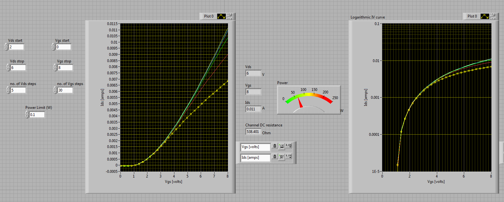
Now let us run NMOS Ids-Vgs. Just download the program
here. Click Run.Save a screen shot for NMOS Ids-Vgs. It should look as shown below in Figure 5.

Figure 5: NMOS Ids-Vgs curve.
What to do in the lab report
Submit all screen shots.
Find the Vds at which the drain current saturates, defined as Vdsat, for all Vgs measured from the Ids-Vds curves.
Compare measured Vdsat with 1st order theory, i.e. Vdsat = Vgs-Vtn. Estimate Vtn from Ids-Vgs curves.
7.6.2. Ids-Vds and Ids-Vgs Using Custom Labview Program for PMOS
7.6.2.1. PMOS Ids-Vds Characteristics
Power off the ELVIS breadboard.
Remove all the connections to the ALD1105 chip (shown in the dashed box in Figure 3).

Figure 6: Circuit connections for PMOS Id-Vgs and Id-Vds measurements. Notice that there are two chips here RC4558(Opamp) and ALD1105 (PMOS).
Proceed as shown in Figure 6. Connect AO1 to the PMOS gate (pin 6), connect the current meter common terminal to the PMOS drain (pin 5), and connect the PMOS source and body (pins 7 and 11) to ground.
Open the LabVIEW program provided
here.Use the following settings:
Vgs start = -2V, Vgs stop = -6V, no. of Vgs steps = 5
Vds start = 0V, Vds stop = -8V, no. of Vds steps = 30
Power on the ELVIS II board.
Click run.
Save a screenshot. It should look as shown in Figure 7.

Figure 7: PMOS Ids-Vds curve.
7.6.2.2. PMOS Ids-Vgs Characteristics
Now let us run PMOS Ids-Vgs. Just download the program
here. Click Run.Save a screen shot for PMOS Ids-Vgs. It should look as shown in Figure 8.

Figure 8: PMOS Ids-Vgs curve.
What to do in the lab report
Submit all screen shots.
Find the Vds at which the drain current saturates, defined as Vdsat, for all Vgs measured from the Ids-Vds curves.
Compare measured Vdsat with 1st order theory, i.e. Vdsat = Vgs-Vtp. Estimate Vtp from Ids-Vgs curves.
7.6.3. CMOS Inverter
Let us now construct and test a CMOS inverter from scratch using the ALD1105. Proceed as follows:
Make sure the ELVIS II power is turned off.
Construct the circuit shown in figure 9 using the pin-level diagram from the pre-lab.
Connect the Analog Input (AI) Channels as shown in the diagram.
Power on the ELVIS II board.
Open the Function Generator SFP and VPS SFP, click Run on both panels.
Set the Frequency to 5 Hz, the VPP to 5V, and the DC offset to 2.5V. Select square wave. The VPP and DC offset combination gives a voltage low of 0 and voltage high of 5V. Set the VPS+ to 5V also.
Note
It is important to notice that the DC offset should always be 1/2 the Vpp. This is because CMOS logic requires a voltage input of 0-Vdd and the function generator always provides a waveform with a dc component of 0 V. That is, “positive” peak is at Vpp/2, and “negative” peak is at -Vpp/2. Therefore, it is necessary to always provide an offset equal to 1/2 Vpp to move the “negative” peak, or the voltage low to 0..
Open the Scope SFP and click Run. Your output should look similar to figure 10.
Adjust frequency until you can see a clear rise and fall of the output signal. Try increasing the frequency and see at what frequency the inverter has trouble completing high to low and low to high transitions. Take screen shots.
Vary VPS+ and FGEN settings to test the same CMOS inverter for VDD=3V. Take screen shots.
Note
The FGEN amplitude should always match the VPS+ voltage.
Vary VPS+ and FGEN settings to test the same CMOS inverter for VDD=7V. Take screen shots.
The inverter will be used in the next part.
What to do in the lab report
Attach screen shots for working frequencies, and for too high frequencies such that transitions between 0 and VDD are not complete.
Attach screen shots for different VDD.
Discuss the impact of VDD on the low-to-high delay and high-to-low delay of the inverter.
7.6.4. CMOS Inverter Voltage Transfer Curve
Now the voltage transfer curve of the inverter will be measured using a customized LabVIEW program.
Remove the capacitor from the previous step.
Set your VPS+ to 5V so that the CMOS inverter sees a VDD of 5V.
Connect the input of the inverter to AO0 instead of FGEN, as shown in figure 11.

Figure 11: CMOS inverter schematic for voltage transfer measurement.
Download the LabVIEW program
here.- Use the following settings:
Vin start = 0v, Vin stop = 5v, nsteps = 30
Save a screenshot of the graph.
Right click on the graph and export the data for later analysis.
(Optional) You can also try different VDD by changing VPS+ and the stop value of your Vin sweep. You will see how the voltage transfer curve changes with VDD.
What to do in the lab report
Show 1 screenshot.
At what input voltage does the output transition to logic low?

