3. PN Junction
3.1. Objectives
- Understand relationships between various potentials and energies important for understanding device operation
- Understand how biasing affects various potentials and energies at device terminals / ohmic contacts
- Understand how carrier concentrations change in response to applied voltage
- Understand how to extract meaningful understanding from data - in this case, simulated data using state-of-the-art tools, Sentaurus Device.
3.2. Overview
We have discussed first order PN junction theory in class. Our class notes also have plenty of information on the fundamentals, and there are plenty of books that discuss PN junctions at varying depths. Most if not all existing treatments use long base diodes, often without stating or realizing the long base assumption. For new students, if you do not know what long base is, that is fine. We will get to that soon. Base in modern transistors, however, is electrically short, meaning recombination is negligible. The band diagrams look nothing like what you see in books. In this lecture, we look at a concrete numerical example of a short base PN junction using Technology Computer-Aided-Design (TCAD).
3.2.1. Why TCAD?
What does TCAD offer us? Take the pn junction problem as an example. If we do not make assumptions on constancy of majority carrier Fermi level, we will have to solve semiconductor equations numerically - it is one of the most difficult computational math problems on earth. There are commercial tools, called TCAD tools, developed specifically for this. They are widely used in the semiconductor industry in designing devices. However, they are much more difficult to use than circuit simulators, and require special knowledge of semiconductor physics, device physics, computational mathematics and of course specific computer programming specific to each tool.
Starting from version 2013, we can no longer visualize 1D structures due to limitation of the new visualization tool. This greatly complicates everything, and 2D is now a necessity. I have done the simulations for you and created plots that will help you understand complex pn junction operations. I am still working toward a solution that will enable you to run some of these simulations yourself.
It is extremely helpful to look at the “accurate” solution which can give us great insight into internal device operation beyond what first order theories can offer us. Inspection of internal quantities allows us to quantify approximations we make, for instance, how quasi Fermi level should vary across the whole PN junction from p-contact to n-contact, how minority carrier concentration is injected, how values of minority carrier concentration at injection points change with bias, how minority carrier concentration vary from the injection point to the exit, the contacts that is.
3.2.2. Study Guide
Study each figure and see if everything makes sense to you. Each plot is carefully designed to show a particular physics. Print out the plots and sketch on them as you read through the text. You can click on individual plot and just print that plot in a separate browser window. Let me know of any mistakes you spot. For best results, you should read the relevant pages in our Onenote notes on pn junction first before reading this.
I intentionally used large size for pictures so details can be seen clearly on a 1080p screen, particularly for band diagrams and composite graphs that contain many plots. To see pictures without blurring, simply set zooming in your browser to 100%.
3.3. Device Structure
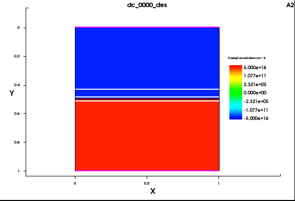
The PN junctionstructure was shown earlier when introducing band diagram drawing of pn junctions. Let us look at the device structure again shown in figure 1.
Doping is Nd=5e16/cm^3 and Na=5e16/cm^3. An abrupt change in the middle occurs. This 0.5um corresponds to “0” in our analytical treatment, that is, the junction interface. It is however, inconvenient to set this point to “0” in TCAD.
3.4. Zero Bias
3.4.1. Band Diagrams
figure 2 shows band diagrams at 0V. The quasi Fermi potentials at all contacts are simply equal to the applied voltages. Since we are applying zero voltages at both contacts, the quasi Fermi potentials are zero.
Quasi Fermi energy is simply the inverse of quasi Fermi potential, if you use eV for energy, and V for potential.
There is built-in potential between the N-contact and the p-contact. Potential is higher at the n-contact, lower at the p-contact.
Therefore, the Ec at the n-contact is lower than the Ec at the p-contact.
Imagine an electron standing at the boundary between neutral region (NR) and transition region (TR) on the n-side, it sees an energy barrier, preventing net diffusion of electrons from n-side to p-side. Imagine an electron inside the TR, the tendency to drift downhill cancels the tendency to diffusion from high concentration (n-side) to low concentration (p-side). The situation for holes is similar.
3.4.2. Electrostatic potential
Now let us add potential to our band diagram. figure 3 shows electrostatic potential on the band diagrams. Unit for potential is V instead of eV. Recall potential reference is that of an intrinsic material. Potential is thus negative at the p-contact, and positive at the n-contact.
Even if we have zero bias at all terminals, there is still built-in potential. The most convenient reference is a piece of intrinsic semiconductor in TCAD. Hand analysis in textbooks, however, uses different reference. This is very important to note so that you know precisely how to associate simulation results with first order theories in textbooks.
3.4.3. eDensity and hDensity
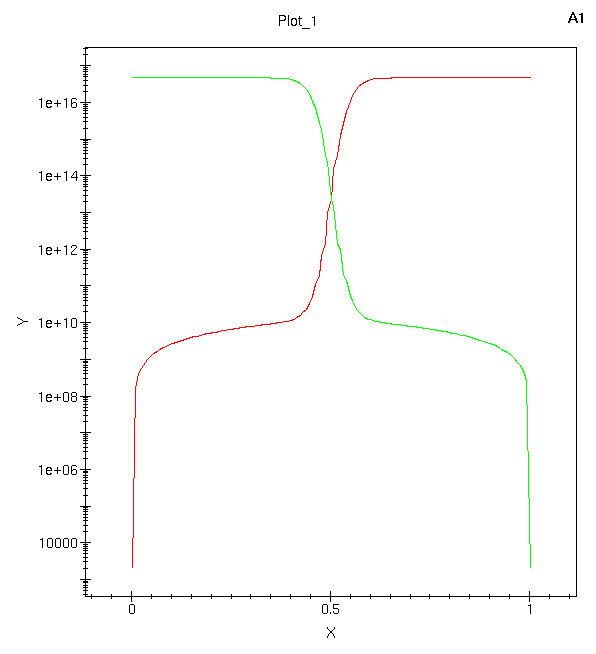
Based on the band diagram, you can easily picture how electron concentration n and hole concentration p vary.
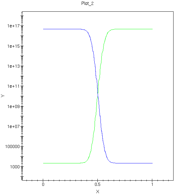
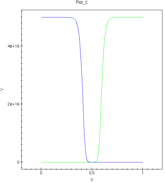
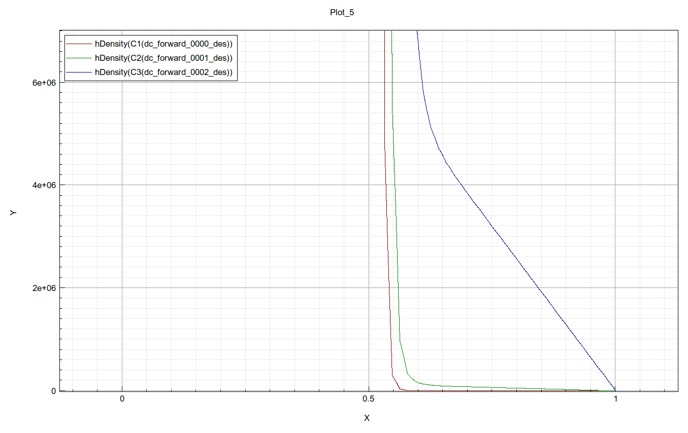
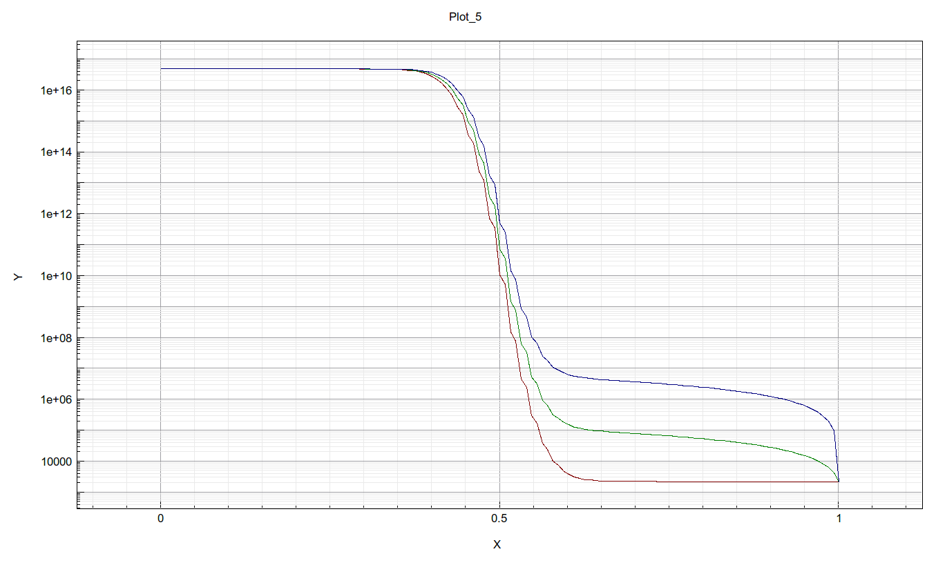
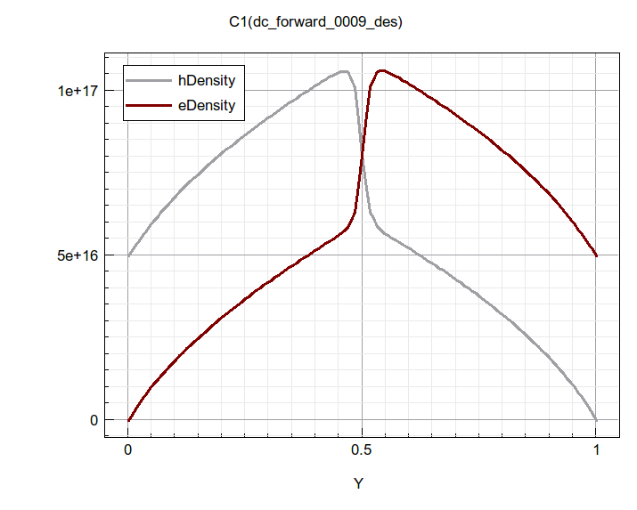
Sketch that yourself, then compare with the following plots shown in figure 4 and figure 5:
Why do we need log scale and linear scale plots? What are the advantages of each type of plot?
3.4.4. Key internal details put together
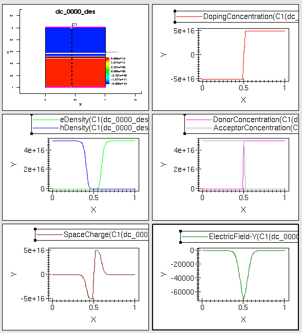
Key internal details are put together in figure 6:
Observe how Nd and Na vary, p and n vary across the junction, then sketch how the net charge density varies yourself. Compare to the SpaceCharge plot. Sketch the space charge from standard textbook depletion approximation as well.
From the space charge density plot, with Gauss’s law and proper boundary conditions of having zero electric field in the far away (from junction interface) regions, we can sketch electric field plot:
- it is negative,
- with slope determined by charge density,
- a maximum occurs at junction interface.
3.5. Forward Bias
3.5.1. I-V Curve
The p-contact electron and hole currents and total current versus p-contact voltage are shown below in figure 7:
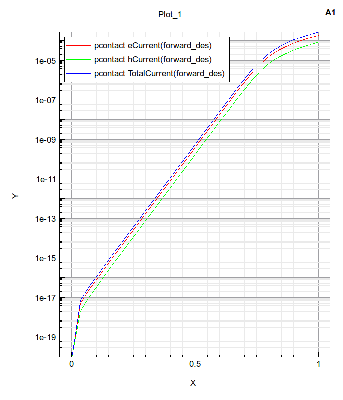
Figure 7: Forward Jn, Jp and J at p-contact versus applied p-contact voltage. N-contact is grounded.
You can indeed verify that at relatively lower bias, below 0.7V, all 3 currents follow closely an exp(qVf/kT) voltage dependence.
However, at higher Vf, the I-V curve starts to bend over for a number of reasons we will see below.
Getting the I-V curve does not tell us much about how the device works. With TCAD tools, we can inspect the internal physics by properly plotting out various physical quantities such as energies, potential, p, n, electric field, current densities for electrons and holes etc.
3.5.2. Operation at low forward biases
3.5.2.1. Band diagrams
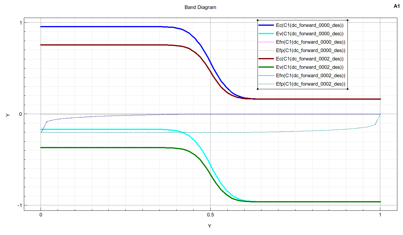
To see effect of bias, let us compare band diagrams at 0V, or equilibrium, with band diagrams at 0.2V p-contact bias, as shown in figure 8:
You should compare this with Shockley theory and see if that theory / our analysis holds. Click on the plot to open it in a new browser window. Print it out, and use your pen to “draw” what you read below on the diagrams.
Efn and Efp, or simply the Ef at the n-contact remains at 0eV with forward bias, as the n-contact is grounded.
The p-contact Ef is pulled down to -qV(p-contact), i.e. -0.2eV for V(p-contact)=0.2V.
As the relative position of Ef in the bandgap does not change at an ohmic contact, which is required to keep p and n at their equilibrium values, Ec at the p-contact has to come down as well by the same amount.
Ec and Ev variation is nearly zero in the QNR. That is most of the potential drop occurs in the TR, where carrier concentration is relatively low compared to the QNRs.
This decrease of Ec at the p-contact also means an increase of electrostatic potential of the p-contact by V(p-contact). We have basically proved this without writing down a single equation. An inspection of band diagram does the job just fine. It is good to be able to read band diagrams.
Mark Efn in the n-side QNR and TR, and note it is virtually constant.
Imagine an electron standing at the boundary between QNR and TR on the n-side, it sees an energy barrier, indicative of an electric field, preventing net diffusion of electrons from n-side to p-side. Remember electrons tend to drift downhill.
A forward bias lowers that barrier, or reduces the opposing electric field, allowing net diffusion of electrons from n-side to p-side.
Consequently, electron concentration increases on the p-side, except for at the p-contact. This is also easily seen by the decrease of Ec-Efn in the TR and p-side QNR with increasing forward bias. The process is called minority carrier injection, as electrons, minority carriers on the p-side, are injected from n-side.
The boundary between p-side QNR and TR, approximately at 0.4um, is called the “electron injection point,” where Efn-Efp is qVf by inspection of the band diagram. Mark Efn-Efp at this point for Vf=0.2V.
pn = ni^2*exp(qVf/kT) in the TR, and of course at this injection point.
At low injection, majority carrier concentration, p on the p-side, remains close to equilibrium value, which we denote as pp0, with first p indicating hole concentration, second p indicating it is p-side, and 0 meaning 0 bias.
Thus n(electron injection point) = ni^2*exp(qVf/kT)/pp0 = np0 * exp(qVf/kT). np0 means “n” on the “p-side” at 0 bias.
A similar situation exists for holes. The energy barrier for hole diffusion from p-side to n-side is reduced by forward bias, causing net diffusion of holes to the n-side, where they are minority carriers.
Just remember all energies on an energy diagram are for electrons. So flip the energy axis when thinking about energy barrier for holes. Going downward means an increase of energy for holes. p(hole injection point) = pn0 * exp(qVf/kT).
Both electron and hole currents flow from p-side to n-side.
This is consistent with what we expect from Jn=n*mun*dEfn/dx and Jp=p*mup*dEfp/dx, as Efn and Efp increase from p-contact to n-contact.
3.5.2.2. Exercises
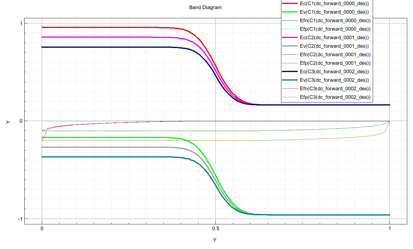
let us compare band diagrams at 0V, or equilibrium, with band diagrams at 0.1 and 0.2V, as shown in figure 9:
See if you can repeat the observations we made earlier with only 0 and 0.2V.
To better see how Efn and Efp change, I have made a plot with only Efn and Efp. See if all curves make sense to you. Again Efp=Efn=0 for 0 bias. So there are only 5 instead of 6 distinct curves as shown in figure 10:
At ohmic contacts, no deviation from equilibrium is allowed. This means that both n and p values are kept at their equilibrium values, determined by doping at the contacts. Efn and Efp must then be equal at the contact points.
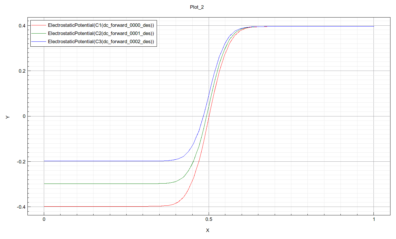
Let us plot out electrostatic potential for the same 3 biases, 0, 0.1 and 0.2V, as shown in figure 11:
Clearly, p-contact potential increases as Vf increases, while n-contact potential stays at its equilibrium value.
3.5.2.3. Minority carrier injection
As we explained using the band diagram, forward biasing causes injection of holes from p to n-side, and injection of electrons from n-side to p-side.
This is best seen on a p and n vs position plot as shown in figure 12:
Can you identify the minority carrier injection points on this graph? In the QNRs, minority carriers move by diffusion, and minority carrier diffusion current is continuous and needs to be spatially constant assuming no recombination, in order to maintain a spatially constant diffusion current. Thus, minority carrier concentration in the QNR should decrease in a linear fashion. The question is that, are we really seeing a linear decrease of minority carrier concentration from injection point to contact?
You may start questioning Shockley theory, how do I see the nice linear distribution of minority carrier in the neutral region? What is going on? It is actually correctly represented on this plot.
We have to switch to linear scale, the chance is you will still not see anything close to a linear distribution of minority carrier if you are using the default axis limits. Think about why.
Then set the y-axis top value to something similar to what you read / or expected from Shockley theory for minority carrier concentration at injection point, as shown below for 0.2V, you will find a very close to linear distribution of the injected minority holes on the n-side, as shown in figure 13.
Indeed you see the straight line. This is also an excellent example of how to inspect your data with plots, just plotting out raw data as is very often is not very helpful or useful even. Same data, on log scale, look like that shown in figure 14.
3.5.2.4. Potential, Ef, p and n at contacts
If we simply set the Ef at the contacts to -q*(applied bias voltage), we can prove that the electrostatic potential at a contact must then be equal to the applied voltage + the built-in potential of that contact with respect to an intrinsic reference. The (quasi) Fermi potentials at the contacts are therefore simply equal to their applied voltage values.
3.5.3. Forward bias at 0.4V
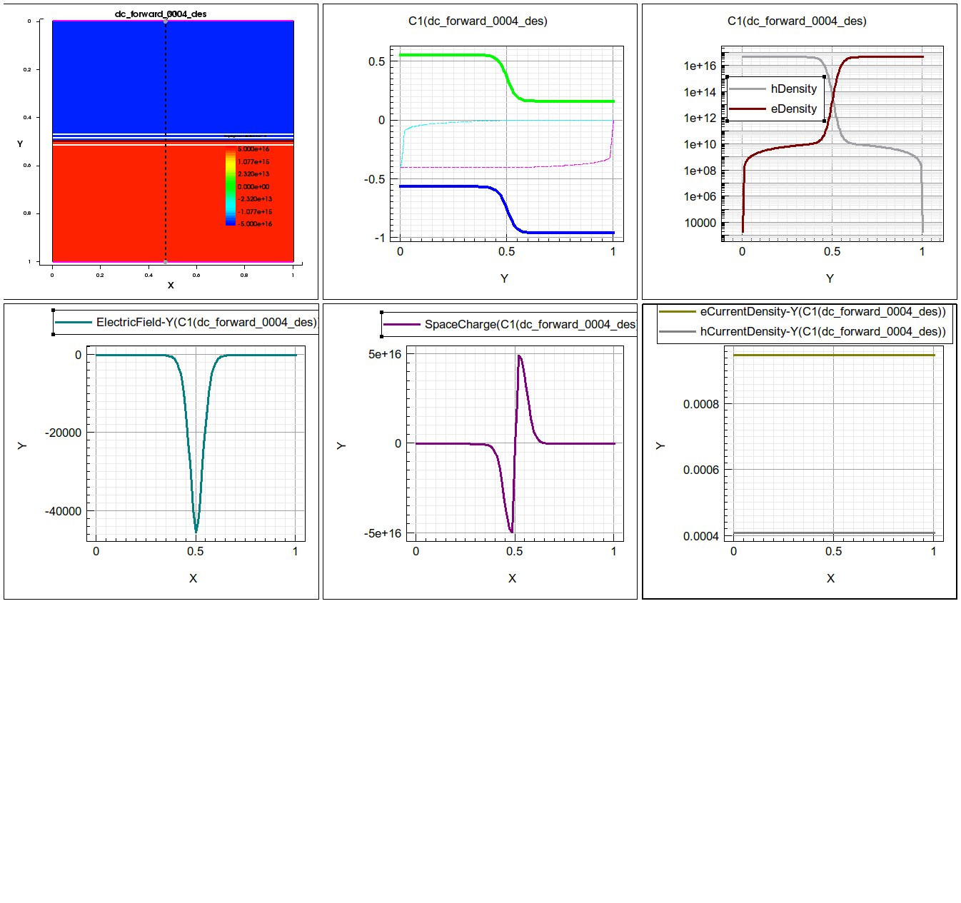
Key internals at 0.4V are plotted below in figure 15.
You should be able to tell from the band diagram that a 0.4V forward bias is applied at p-contact, and n-contact is grounded. Observe:
- e-field close to triangle near the middle, but with soft transition
- Space charge density peak is close to -qNa and +qNd in transition region, but the shape is not quite “rectangular” like you see in many books, no matter how reasonable many of the “justifications” for depletion approximation sound like. In reality, it is NOT a very good approximation in forward mode, even for modest biases. However, it is qualitatively simple and thus useful for intuitive understanding. In fact, this “depletion” approximation becomes worse and worse with increasing bias.
- Jn and Jp are spatially constant (continuous).
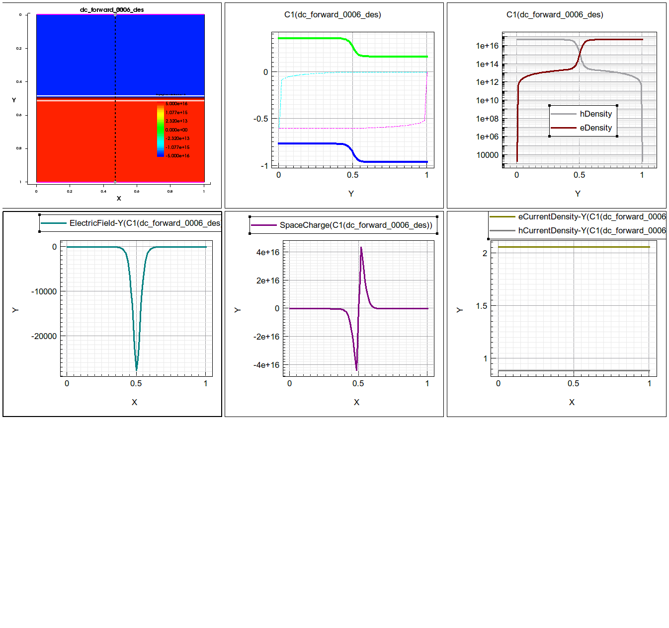
One more example is given below for 0.6V p-contact voltage in figure 16.
See if you can make some observations of your own. See how much Jn and Jp have increased compared to Vf=0.4V.
3.6. High Bias Effects
3.6.1. Internal Details at 0.9V
The key to our low injection theory is the assumptions we made on constancy of majority carrier quasi Fermi level through the quasi neutral regions (QNR), as well as the transition region (TR).
Basic physics says dEfn/dx and dEfp/dx increase with
increasing current.  .
.
At high enough current, dEfn/dx and dEfp/dx will be high, eventually we cannot ignore the variation of Efn in n-region and variation of Efp in p-region, or even the transition region.
This will also cause a sizable amount of e-field in the quasi-neutral regions - which is reflected on Ec and Ev, as shown below for a forward bias of 0.9V, which is in fact, higher than the built-in potential of the junction, in figure 17.
Observe that the e-field is positive in quasi neutral region, and it is NOT spatially constant like in a regular resistor.
You may to first order understand this as a voltage drop over the series resistance of the quasi neutral regions, as you will see from the band diagrams.
Depletion approximation becomes totally invalid of course. The e-field distribution becomes much more complicated. You will have positive electric field (as opposed to “0” at low injection) in the neutral regions, and negative electric field in the transition region.
The space charge density is certainly no longer -qNa on p-side and +qNd on n-side of the TR. In fact, it is much less.
Jn and Jp are quite high, but not as high as low-injection theory would predict.
One reason is Efn-Efp at injection points is now less than qVf.
We should also notice that minority carrier drift current is also no longer negligible.
Quasi charge neutrality is still okay - you can see that injected minority carrier has induced extra majority carrier - making majority carrier concentration (p on p-side, n on n-side) obviously higher than equilibrium ( p=Na on p-side, n=Nd on n-side), as shown in figure 18.
This means that in the quasi neutral regions, a voltage increase causes increase of both p and n, to external circuit, this means capacitance.
This capacitance has to do with minority carrier injection and diffusion, so it is called “diffusion capacitance”. We will come back to this.
This of course exists at low injection too, however, it is impossible to directly observe the change in majority carrier concentration, simply because it is too small compared to majority carrier concentration.
Solving equations in frequency domain is necessary to model general small signal behavior.
3.6.2. Neutral Region Electric Field vs Bias:
If we repeat the above process for many more forward voltages in small step, then plot out the e-field at say the p-contact, we can get a good picture of how the e-field in the quasi neutral regions build up at higher voltage and current. I have done this for you in figure 19.

Figure 19: Forward current and the field at p-contact versus p-contact voltages. N-contact is at 0V.
The 2nd plot has the e-field at p-contact plotted as a function of forward voltage. When the e-field at the p-contact starts to increase, the I-V curve bends over.
Again, to first order, you might think of it as a result of passing a current through a resistive region, once current is high enough, I*R product becomes significant. Recall how Efn, Efp, and Ec vary in a resistor? Here, the voltage drop on the n-side is measured by Efn variation, while the voltage drop on the p-side is measured by Efp variation.
Obviously at high injection, n is no longer spatially constant in the n-region, p is no longer spatially constant in the p-region. Thus dEfn/dx in n-region and dEfp/dx in p-region are no longer spatially constant, and they both change as a function of bias.
Thus simply adding a regular resistor is not a perfect way of “modeling” or “explaining” the I-V curve bending, something I should emphasize, but it works fine in practice and serves as the physical basis of modeling diode as the series of an ideal Shockley diode with a regular ohmic resistor in circuit simulators (SPICE like).
Another problem is that it does NOT allow modeling of the deviation of minority concentration at injection point from exp((efn-efp) /kT) - think about why (and bonus problem in our homework) first.
See our Onenote notes on high injection for more equations and explanations on this point.
