Operation of PN Junctions and Reinvention of Bipolar Transistors
Use the navigation pane on the right hand side of your browser window for easier navigation.
Essential Physics
The essence of bipolar transistor operation is minority carrier injection.
A perfect balance of drift and diffusion exists for both electrons and holes in the transition region of a PN junction under zero bias, or equilibrium. Now let us consider what happens to this balance when an external bias is applied, and how a forward bias causes injection of electrons to the p-side, and injection of holoes to the n-side. As a result, concentration of electrons is increased on the p-side, concentration of holes is increased on the n-side, which is why this process is called minority carrier injection.
Forward Biased PN Junction
The built-in field points from the n-side to the p-side, as field lines originate from positively charged ionized donors, and terminate at negatively charged ionized acceptors.
Consider applying forward bias,  , defined as p-side minus n-side voltage
difference.
The applied field is opposite to the built-in field, as shown below,
thus weakening drift, and causing
net diffusion of holes from p-side to n-side, and
net diffusion of electrons from n-side to p-side.
Electrons, minority carrier on the p-side, are said to be injected (from the n-side).
Holes, minority carrier on the n-side, are said to be injected (from the p-side).
, defined as p-side minus n-side voltage
difference.
The applied field is opposite to the built-in field, as shown below,
thus weakening drift, and causing
net diffusion of holes from p-side to n-side, and
net diffusion of electrons from n-side to p-side.
Electrons, minority carrier on the p-side, are said to be injected (from the n-side).
Holes, minority carrier on the n-side, are said to be injected (from the p-side).

Figure 1: forward biased pn junction
There are lots of holes on p-side, lots of electrons on the n-side,
so this current can be very large with sufficient forward bias. In fact, the
forward current increases exponentially with  ,
with
,
with  being the thermal voltage, approximately 25 mV at 300K.
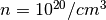
Reverse Biased PN Junction
If  , the junction is said to be under reverse bias.
The applied field is the same direction as the built-in field, as shown below:
, the junction is said to be under reverse bias.
The applied field is the same direction as the built-in field, as shown below:

Figure 2: reverse biased pn junction
Therefore, drift dominates diffusion, true for both electrons and holes. A net current will then flow from n-side to p-side, intuitively satisfying.
The reverse current, however, is very small in magnitude. Electrons drift against field, that is, from p-side to n-side. However, on the p-side, electrons are in minority, and thus we have a lack of electron supply. Similarly, holes drift along field, from n-side to p-side, but there are very few holes on the n-side.
Reverse Biased PN Junction can Pass Current!
Reverse biased PN junction can actually pass as much current as a forward biased PN junction can! This is precisely how we make transistors out of PN junctions, as illustrated below.
The key is that a reverse biased junction does not pass current because of lack of supplies. If we use a forward biased PN junction to supply electrons to the p-side of a reverse biased PN junction, all of these electrons will pass through the reversed PN junction. This configuration is known as a “NPN” transistor.
For example, at equilbrium, if 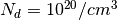 on the n-side,
 n=, but
 ,
as governed by the mass action law
,
as governed by the mass action law  , with
 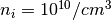 .
It is easy to see why reverse current of PN junction is small.
.
It is easy to see why reverse current of PN junction is small.
We have distinguished electron and hole currents in a PN junction. From a circuit standpoint, once these currents come out of the device, they both become electron current in the metal wire. So what is the point of evening distinguishing them if we cannot separate them?
Now think about inventing a device that can separate electron and hole currents. A transistor does exactly that.
Bipolar Transistor Operation
Consider a forward biased junction (N on left side, P on right - still a PN junction), and reverse biased junction, large current flows in the forward PN, and little current flows in the reverse biased PN. Then bring them close, so the p-regions become a single p-region, we can now make the reverse biased junction flow a lot of current!
Figure 3: essence of transistor action
The reverse biased junction has a very strong e-field. This e-field sweeps (attracts) electrons to the n-side of the 2nd N-region, but is not attractive to holes at all. This keeps electron density very low at the end of the p-region. For all practical purposes, this e-field is a sink for electrons like a contact is.
We now have separated electron current from hole current in the forward biased PN junction.
The first N-region is called emitter (of electrons) as it emits electrons, the 2nd N-region is called collector (of electrons) as it collects electrons.
The p-region is called base for historical reasons. An NPN bipolar transistor is reborn! We can redraw the previous transistor operation illustration using transistor terminologies as follows:

Figure 4: forward active mode transistor operation and equivalent circuit
We can engineer the doping levels / width of base, emitter to make collector current much larger than collector current to realize current amplification.
Transistor Under General Biases
Electron and Hole Current Flows
Under general biases, we will need to consider the minority carrier concentration profiles modulated by the two junction biases, VBE and VBC, respectively. From Shockley theory, minority carrier concentration is modulated by an expoential factor at the injection points, i.e. the boundary between depletion and neutral regions, as shown below:
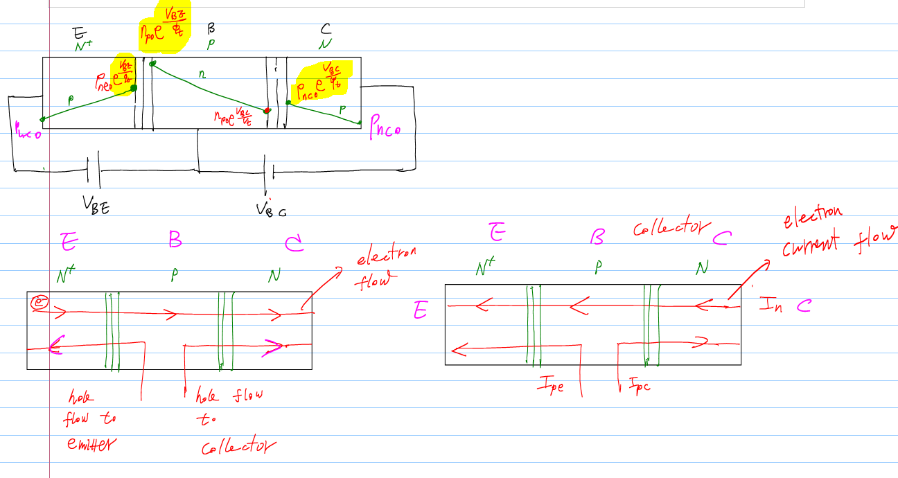
Figure 5: transistor under arbitrary VBE and VBC biases
We will have two hole currents, due to injection of holes from the p-type base, to the n-type emitter and collector.
To which direction electrons flow will depend on if VBE or VBC is higher. If VBE > VBC, electrons diffuse from E to C, and electron current flows from C to E.
The electron diffusion current that flows from C to E can then be calculated as follows:
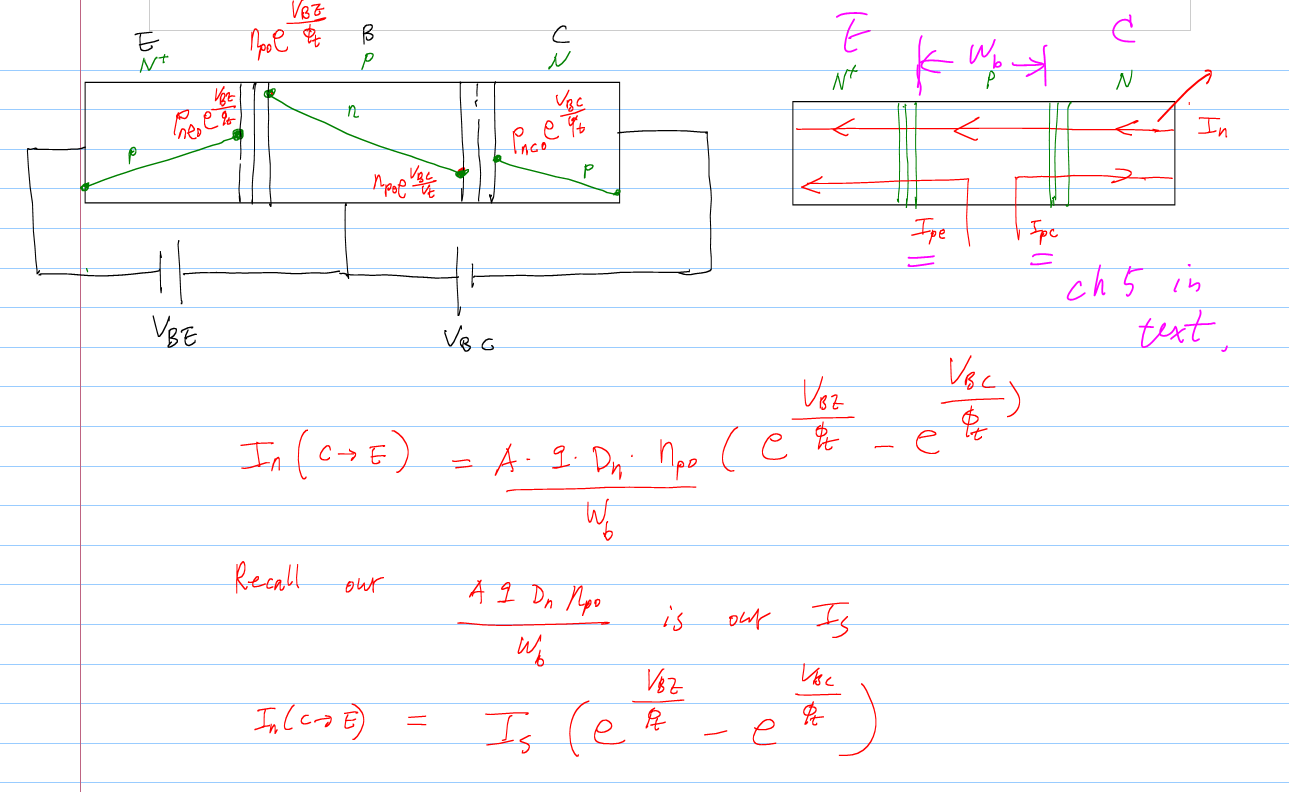
Figure 6: calculation of electron transport current between C and E for arbitrary VBE and VBC biases
The two hole diffusion currents that flow from B to E and from B to C can be calculated similarly.
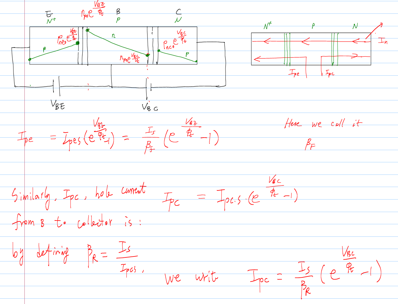
Figure 7: hole current from B to E, and from B to E for arbitrary VBE and VBC biases
We often express the saturation currents of the hole currents using the saturation current of the main electron current, with two ratios, BF and BR. They are called the forward and reverse current gain.
Operation Modes
Forward Active Mode
When VBE > 0, VBC <0, transistor works in forward mode. Collector current IC is mainly electron current injected from the emitter. Base current is mainly hole current injected into the emitter from the base. A small change in VBE which controls IB also produces a large change in IC.
Reverse Mode
When VBC >0, VBE <0, transistors works in reverse mode.
Saturation Mode
When VBE >0 and VBC >0, transistor works in saturation mode. VCE = VCB + VBE = -VBC + VBE is small, around 0.2V or so for practical transistors. A large amount of current can still flow between C and E. The effective resistance between C and E is thus small, and transistor acts as a closed switch.
Cutoff Mode
When VBE <0 and VBC < 0, transistor works in cutoff mode. There is no significant current anyhow.
Operation Modes in Practice
The above definitions are highly simplistic, and do not really represent how we use transistors in real circuits. For instance, a VBE of 0.5V and a VBC of -2V will not give much useful current, and it is really a cutoff condition for most practical circuits.
Another example is that a VBE of 0.8V and a VCE of 0.3V will fall into saturation mode if you follow the standard textbook definition, but in reality, the forward VBC (0.5V) is insignificant compared to VBE (0.8V) in determining the electron transport current between C and E. This is really in forward active mode. We indeed use such bias in amplifiers, particularly with a low power supply voltage as low as 1V.