
Auburn University offers clean room laboratories for microelectronics and electronics packaging research
Auburn University has extensive microelectronics, electronics and packaging capabilities from design to implementation. Within the Department of Electrical and Computer Engineering, there is approximately 8,500 square feet of laboratory space dedicated to microsystems development and testing, including integrated circuit and MEMS device fabrication, thick film hybrids fabrication, die and component level packaging, circuit board assembly, environmental testing and failure analysis.
Additional capabilities include extensive software tools and CAD applications for microsystem design and simulation and development, including Synopsis, Mentor Graphics, IntelliSuite, CoventorWare, OrCAD, Zemax, Lavenir, Lasi and AutoCAD. Auburn University's microsystems capabilities cover not only the microdevice design and fabrication, but also the design and implementation of the support electronics and software necessary for integrating microdevices and microsystems into useful end applications.
Recent projects include:
- Electronics for a Mars rover that meets the temperature requirements of -180 degrees Celsius to 120 degrees Celsius. This will allow the rover to explore regions previously unreachable due to temperature extremes and/or lack of solar energy used to heat the electronics.
- Extreme temperature rectifiers utilizing Auburn's research efforts in carbon nanotube growth and packaging. These rectifiers will be used at temperatures as high as 1,000 degrees Celsius, far exceeding the standard 200 degrees Celsius maximum for silicon rectifiers. Applications of these rectifiers include electronics for deep well drilling and jet engine monitoring.
- Researchers are also investigating the other end of the temperature range, exploring packaging components that perform at temperatures as low as 10 Millikelvin – that's 0.01 Kelvin (room temperature is 293 Kelvin).
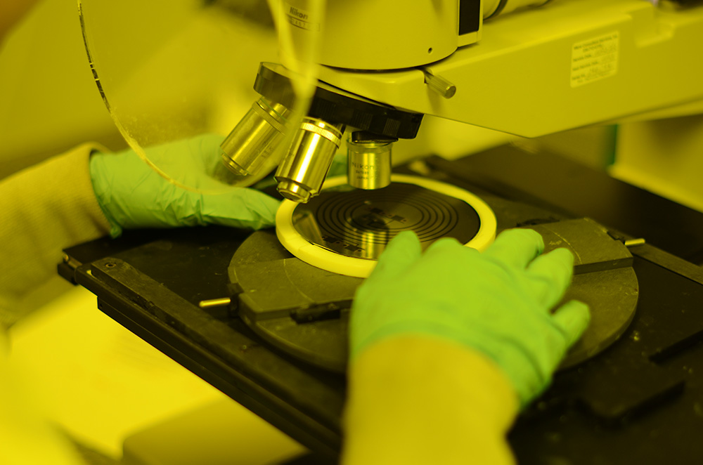
Auburn University's microfabrication capabilities include: Two STS ASE DRIEs, two sets of oxidation/diffusion furnaces, STS PECVD system (low temp oxide and nitride), 7 E-beam target + 1 sputter target vapor deposition system with dual E-gun capability for co-deposition, Karl Suss MA/BA 6 frontside/backside contact mask/bond aligner, Strasbaugh CMP system, Okamoto wafer grinder, ellipsometers and laser reflectometer, IR interferometer, pulse tube cryostat, and cryo probestation. Processes include AOE deep oxide etch, anodic bonding, polyimide curing, wet processing (including HF release), CPD and copper/gold/silver/ni plating.


